GeForceFX: NVIDIA goes Hollywood?
Get Tom's Hardware's best news and in-depth reviews, straight to your inbox.
You are now subscribed
Your newsletter sign-up was successful
DDR-II Memory & Memory Interface
DDR memory has recently become a standard feature among mainstream and even budget cards. DDR stands for double data rate, and describes memory that can transfer data both on the rising and the falling edge of a clock signal. The result is a twofold increase in the theoretical maximum data bandwidth and throughput without a corresponding increase in clock speed. DDR memory employs two-bit prefetches, each of which can send two bits of information to the memory via a data path. DDR-II now uses a four-bit prefetch, again doubling the memory throughput. DDR-II also offers some other advantages:
- lower voltages, reduced from 2.5V to 1.8V;
- lower access times between 1,8ns to 2,2ns, down from DDR's 2,9ns;
- termination of the data paths on the memory chip instead of on the PCB (resulting in cleaner signal quality.
All of these factors work together to allow for higher memory clock speeds.
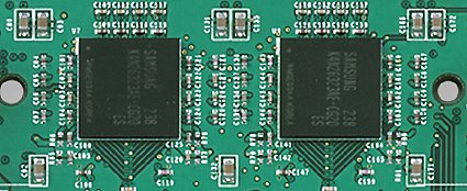
Samsung DDR2 memory modules.
Article continues belowThe memory interface of the GeForceFX has been designed with DDR-II in mind from the start. It will most likely use memory modules clocked at 500 MHz (1 GHz DDR-II) on a 128 bit bus, offering a solid memory bandwidth of about 16 GB/s. While this is an improvement over the GeForce4 Ti's 10.4 GB/s, it's still a far cry from ATi's Radeon 9700 PRO, whose 256 bit DDR memory interface offers a full 19.6 GB/s.
Although higher memory bandwidth is always a good thing, modern graphics cards achieve their high performance by employing intelligent memory interfaces. Matrox' Parhelia is a prime example of this. Even though its theoretical bandwidth is twice as high as that of a GeForce4 Ti4600 (NV25), it fails to achieve its rival's scores by a long shot. The reason is the NV25's highly optimized memory interface (Lightspeed Memory Architecture). The GeForceFX (NV30) will use an even more refined version of this interface. In addition to Z-data compression, the chip is now capable of lossless 4:1 color compression in real-time (more on that later, in the section on Intellisample). NVIDIA promises a major performance-boost in combination with antialiasing. On top of that, larger caches and more refined caches as well as highly tweaked "crossbar" controller are also part of the new chip (see also: PC Graphics Beyond XBOX - NVIDIA Introduces GeForce4 ).
One word on the memory bandwidth of GeForceFX. You can calculate that as follows. Let's begin with some examples:
GeForce4 Ti:
Get Tom's Hardware's best news and in-depth reviews, straight to your inbox.
16 Bytes * 325 MHz * 2 = 10,4 GB/s
The buswidth of the memory is 128 bit which means that 16 Bytes of data can be transfered by clock. Since the DDR memory is using a prefetch of 2, the data rate is doubled. Let's take a look on the Radeon 9700 PRO:
32 Bytes * 310 * 2 = 19,8 GB/s
You have to take 32 Bytes here since the memory bus on the card is 256 bit wide. Now let's see the GeForceFX. The card is using DDR2 memory which means it's using a prefetch of 4 and doubles the amount of data transfered again. If a card is running with 1 GHz DDR2 datarate, the modules can be run at a quarter of that: moderate 250 MHz. That's what people mean when they say that DDR2 is a cheap solution with a lot headroom. You can also read that in the Jedec whitepaper on page 6.
NVIDIA is using Samsung DDR2 modules with a dram cell frequency of 500 MHz - only half the data frequency. This means that the DDR2 memory on GeForceFX behaves just like DDR memory with just higher clock frequencies.
So here we go:
16 Bytes * 500 MHz * 2 = 16 GB/s
This goes common to a Samsung whitepaper on the DDR2 modules NVIDIA is using for the GeForceFX. It says that one module (32 bit) has a single Bandwith of 4 GB/s. This means 16 GB/s for 128 bit. GeForceFX is using 2 banks with 4 modules each - if you wondered after counting the number of chips on the card.
