Intel Core i5 And Core i7: Intel’s Mainstream Magnum Opus
Get Tom's Hardware's best news and in-depth reviews, straight to your inbox.
You are now subscribed
Your newsletter sign-up was successful
QPI, Integrated Memory, PCI Express, And LGA 1156
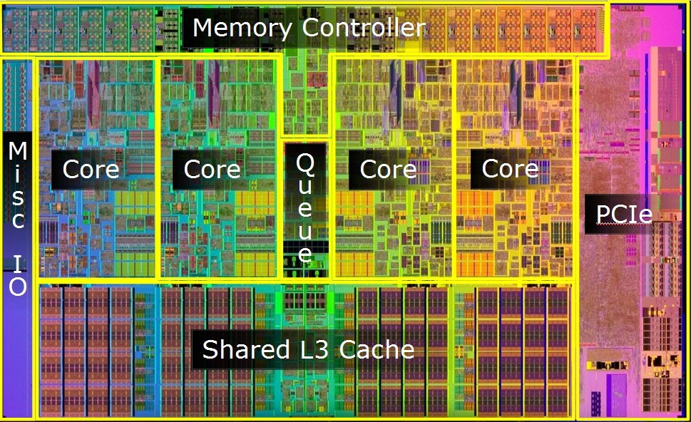
The company won’t get specific about the changes made to its QuickPath Interconnect, the point-to-point interface first used to attach Core i7 to X58. But there is a QPI link inside of Lynnfield, serving as the glue between on-die PCI Express and the uncore. Intel has a lot more freedom with this technology now, since it doesn’t have to leave the die. Thus, the performance and timings are both reportedly better here than they were on Bloomfield.
This interconnect is important today, naturally, but will become a key performance enabler when Clarkdale launches next year. With graphics and memory control on the same piece of silicon, memory bandwidth—one of the biggest Achilles’ heels of integrated graphics designs—is delivered much more effectively. As a result, expect to see Intel adjusting the speed of its internal QPI link up or down to differentiate its Clarkdale SKUs.
Of course, none of that is really a concern with Lynnfield, which employs 16 lanes of integrated PCI Express 2.0 to interface with discrete GPUs. We’ve already spent considerable time comparing the performance of single- and dual- card configurations on P55 against X58, P45, and 790GX using 2.8 GHz processors. We've determined that there’s very little gain or loss resulting from Intel’s Lynnfield implementation. In other words, the integration of PCI Express is just about as close to transparent to end-users as possible. This is the way integration should work (though most of us have been conditioned to think it automatically leads to performance sacrifices).
Article continues belowMuch more impactful is the licensing of SLI and CrossFire, which allows most P55-based motherboards to support either technology, just like X58. Of course, the difference is that P55 platforms are going to be significantly cheaper. More on the chipset shortly.
Finally, you have the processor’s integrated DDR3 memory controller, which is cut from three 64-bit channels in Bloomfield to two 64-bit channels with Lynnfield. Officially, Bloomfield is rated for up to DDR3-1066, yielding a theoretical maximum of 25.6 GB/s of bandwidth. We’ve all seen the LGA 1366-based Core i7s scale as high as DDR3-2133 though, so the official spec means very little to enthusiasts. In contrast, Lynnfield is rated for DDR3-1333 memory modules, offering up to 21.3 GB/s. For the most part, the loss of that third channel is made up for by an increase in attainable data signaling rate. We’ll put this theory to test in a couple of pages.
LGA 1156: More Socket Segmentation
The table below should look somewhat familiar; I used it back in February to chart the last nine years of desktop socket launches from Intel and AMD. With the debut of LGA 1156, the Intel column is looking pretty darned crowded.
Get Tom's Hardware's best news and in-depth reviews, straight to your inbox.
| Disruptive Socket Launches | ||
|---|---|---|
| Year | AMD | Intel |
| 2001 | Row 1 - Cell 1 | Socket 478 |
| 2002 | Row 2 - Cell 1 | Row 2 - Cell 2 |
| 2003 | Socket 754 | Row 3 - Cell 2 |
| 2004 | Socket 939 | LGA 775 |
| 2005 | Row 5 - Cell 1 | Row 5 - Cell 2 |
| 2006 | Socket AM2 | (Intel launches Core 2 Duo, most motherboards need to be replaced) |
| 2007 | Row 7 - Cell 1 | Row 7 - Cell 2 |
| 2008 | Row 8 - Cell 1 | LGA 1366 |
| 2009 | (Socket AM3–new processors work in old motherboards, but not the other way around) | LGA 1156 |
I’m sure there will be a number of enthusiasts who’ve spent a lot of money on LGA 1366, X58, and Core i7. You'll see the performance of Lynnfield, compare the cost, look at the upgrade path to Clarkdale, and ask me why I couldn’t have given a more vocal heads-up about what was to come. To those folks, let me give you one hopefully-welcome piece of information: the upcoming Gulftown design (32nm, hexa-core, Hyper-Threading-enabled) will be a drop-in upgrade to your existing platform. Meanwhile, those waiting on Clarkdale have a dual-core design to look forward to—certainly not as sexy, unless you’re really itching for integrated graphics.
What, then, was the impetus behind LGA 1156 less than a year after LGA 1366? And why couldn’t Intel integrate PCI Express on the LGA 1366 platform, too?
Right from the get-go, 1366 was designed as a DP interface for Intel’s Tylersburg platform. The fact that it surfaced first on the desktop is similar to how LGA 771 made a brief appearance in Intel’s Skull Trail gaming configuration. The difference is that motherboards based on X58 made their way under $200 and the cheapest processors dropping into the interface are less than $300. That’s not little money, to be sure. But it’s affordable enough to tempt the folks who know how fast an overclocked i7 machine can be.
LGA 1366 didn’t get PCI Express because it would have made the pin-out far too complex. Plus, the servers and workstations that now use the 5520 and 5500 chipsets need access to more than just 16 lanes of connectivity for storage controllers, professional graphics cards, and high-speed networking.
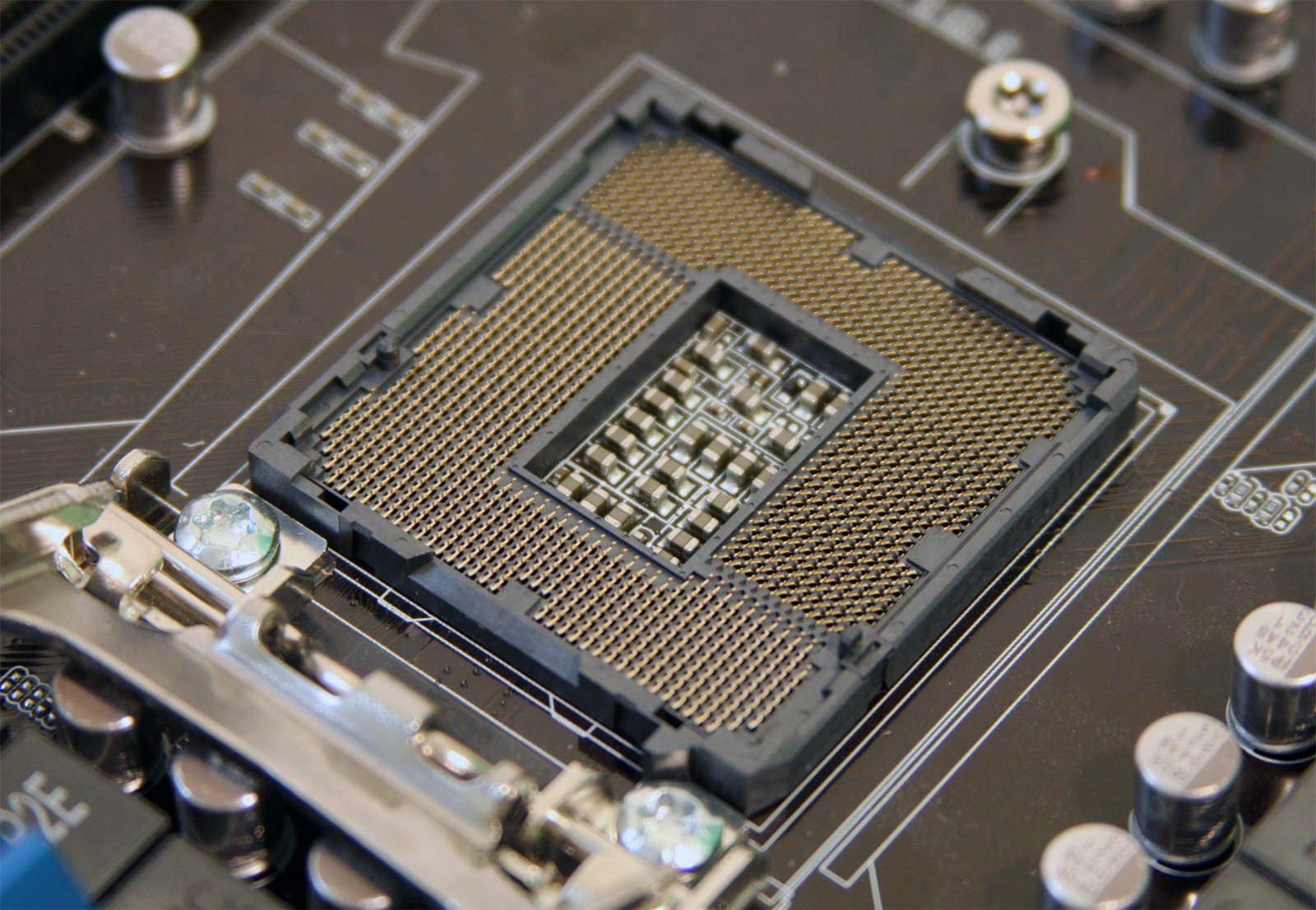
Thus, LGA 1156 becomes the true successor to LGA 775, despite now-convoluted segmentation. It’s simpler than LGA 1366, its locking mechanism applies pressure more evenly on the CPU’s heat spreader, and it helps protect against EMI—particularly important when Clarkdale exposes on-chip graphics.
You can expect this processor interface to remain pervasive until the end of 2011, when LGA 1155 (planned launch in the first half of 2011) starts grabbing market share big time.
Current page: QPI, Integrated Memory, PCI Express, And LGA 1156
Prev Page What’s In A Name? Next Page Intel’s Turbo Boost: Lynnfield Gets Afterburners-
caamsa Dang! AMD better get their $4iT together. Now I need to decided between i7, i5 or phenom II when I do my next upgrade........technology happens too fast. Looking forward to more reviews on the i5 and mb prices.Reply -
People need to be careful when comparing the i7-870 to a i7-920, alot of people pre-release were worried that the 1156 platform was going to dominate the 1366. However when you see the 870 out perform the 920 people need to remember that a 870 is double the price of a 920, and even when you factor in a motherboard a 920 setup comes out cheaper than a 870.Reply
Now the i5 750 on the other hand is great performance at a great price, and would certainly be the budget gamers new weapon of choice.
I currently have an i7-920 setup which is my main rig and am very happy with it and not at all upset to the see the 870 outperform it (since the 870 would cost me twice as much). I also have had an i5 750 setup now for over a week (the 1156 processors and motherboards have been available here in Australia for nearly 2 weeks now) and it is an amazing processor for the price of it.
So what am I trying to say? 1366 is still a good platform for the top end of the market. The i5 are fantastic new processors for their price, and the 1156 i7's are just confusing and I'm not really sure who they are going to appeal to? I could understand it if Intel launched the 1156 i7's in 6months time when alot of users are already using the 1156 platform and are looking to upgrade their CPU without a new mobo. But to anyone looking at getting a 870, just get an 920 and use the extra cash on the mobo and ram to go with it. -
Nintendork A little confusing the charts.Reply
I would prefer a bench with HD4890. They scale better in CF. -
cabose369 Intel needs to come up with a simplified naming system for their products. They are as bad as NVIDIA is right now in terms of naming their products.Reply
There is sooo much to learn and there is so much information here.... I feel confused!! -
alikum Well, I just hope that the Core 2 Quads will drop in prices significantly so that I could grab the high-end one for my final LGA775 upgrade!Reply -
buzznut Well this is good news for consumers. I'm not certain why it took so long for Intel to make some mainstream proc like i5, but for intel fans it seems worth the wait.Reply
This will also compel AMD to bring some more value to the market. Nice article. -
jawshoeaw damn, 150 watts at idle?? Is that just the cpu? I hope the gaming rigs built on these processors are not left on 24/7. My old AMD X2 3800 system including the monitor uses less than 150 watts at idle (50 of which is the 22" LCD).Reply -
unclewebb i7 Turbo is a good tool to monitor the multiplier of Core i5/i7 CPUs.Reply
http://www.fileden.com/files/2008/3/3/1794507/Turbo.zip
It uses the method that Intel recommends in their November 2008 Turbo White Paper. -
evolve60 "Intel Core i7-920 Extreme (Bloomfield) 2.66 GHz, LGA 1366, 4.8 GT/s QPI, 8 MB L3, Power-savings enabled"Reply
Since when has the I7-920 become an extreme?


