Intel Core i5 And Core i7: Intel’s Mainstream Magnum Opus
Get Tom's Hardware's best news and in-depth reviews, straight to your inbox.
You are now subscribed
Your newsletter sign-up was successful
What’s In A Name?
With Core 2 Quad and Core 2 Duo, you had a general idea of what you were dealing with upfront. Adding a Q8000- or E7000-series designator wasn’t particularly descriptive, but at least there was one tangible identifier in there for the layman to digest.
When Intel introduced Core i7 last year, the fact that there was only one Nehalem-based desktop family made it easy to say “Core i7—yeah, high-end stuff,” regardless of whether you were actually talking about the $300 i7-920 or the $1,000 i7-965.
Now you have Core i5 and another strain of Core i7; at this point the nomenclature is just jargon for everyone except for the power users who live and breathe this stuff. Let’s break it down in a neat little table, though.
Article continues below| Header Cell - Column 0 | Core i7 (LGA 1366) | Core i7 (LGA 1156) | Core i5 | Core 2 Quad |
|---|---|---|---|---|
| Processor Interface | LGA 1366 | LGA 1156 | LGA 1156 | LGA 775 |
| Number of Cores | 4 | 4 | 4 | 4 |
| Turbo Boost | Yes | Yes | Yes | No |
| Hyper-Threading | Yes | Yes | No | No |
| L1 Cache | 32KB/32KB per core | 32KB/32KB per core | 32KB/32KB per core | 32KB/32KB per core |
| L2 Cache | 256KB per core | 256KB per core | 256KB per core | Up to 12MB shared |
| L3 Cache | 8MB shared | 8MB shared | 8MB shared | No |
| Memory Channels | 3 | 2 | 2 | 2 |
| Max. Memory Rate | DDR3-1066 | DDR3-1333 | DDR3-1333 | DDR3-1600 |
| Chipset | X58 | P55 | P55 | X48 |
| Price | $284-$999 | $285-$555 | $199 | $163-$316 |
As you can see, Core i7 for LGA 1366 remains the enthusiast-class offering, sporting the most PCI Express 2.0 connectivity via Intel’s X58 Express chipset, up to three available channels of DDR3 memory support, Intel’s first generation of Turbo Boost, and Hyper-Threading.


Core i7 for LGA 1156 integrates the PCI Express connectivity (albeit 16 lanes instead of 36), sheds one memory channel, incorporates an updated implementation of Turbo Boost, and maintains Hyper-Threading support.
Core i5 includes the same on-board PCI Express subsystem and dual-channel integrated memory controller. It employs Intel’s improved Turbo Boost (though it’s slightly less aggressive than i7’s). What it lacks, however, is Hyper-Threading—apparently a noteworthy-enough capability to turn an i7 into an i5. Of course, descending the stack also results in lower base clock rates.
The Making Of A Core i5/i7
Get Tom's Hardware's best news and in-depth reviews, straight to your inbox.
Architecturally, most of what you get in a Core i5 or Core i7 processor is borrowed from technology already found in Intel’s LGA 1366-based Core i7 and Xeon 3500-series processors. The Lynnfield die is different from Bloomfield though, estimated at 774 million transistors packed into 296 square millimeters (versus 731 million in 263 millimeters for the first Core i7s). More than 400 million of those transistors make up the CPU's cache.
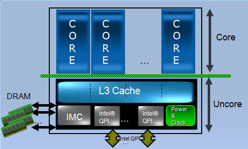
As with Bloomfield, Lynnfield is a monolithic design divided into four cores (execution pipelines, L1 data/instruction cache, TLBs) and the uncore (L3 cache, integrated PCI Express, the memory controller, QPI, and the PLLs). The power for these two “halves” remains separate, independently adjustable in your motherboard's BIOS.
Each of the four cores retains its 32KB L1 data cache (still 8-way set-associative), 32KB L1 instruction cache (still 4-way set-associative), and 256KB L2 cache (you guessed it—still 8-way set associative). An inclusive 8MB L3 cache 16-way set-associative) should look familiar as well.
With nothing really new to report in the cores themselves, we move to the uncore, where Intel has added PCI Express 2.0 connectivity, axed a single memory channel, dropping the total to two, and altered QPI.
Current page: What’s In A Name?
Prev Page Introduction Next Page QPI, Integrated Memory, PCI Express, And LGA 1156-
caamsa Dang! AMD better get their $4iT together. Now I need to decided between i7, i5 or phenom II when I do my next upgrade........technology happens too fast. Looking forward to more reviews on the i5 and mb prices.Reply -
People need to be careful when comparing the i7-870 to a i7-920, alot of people pre-release were worried that the 1156 platform was going to dominate the 1366. However when you see the 870 out perform the 920 people need to remember that a 870 is double the price of a 920, and even when you factor in a motherboard a 920 setup comes out cheaper than a 870.Reply
Now the i5 750 on the other hand is great performance at a great price, and would certainly be the budget gamers new weapon of choice.
I currently have an i7-920 setup which is my main rig and am very happy with it and not at all upset to the see the 870 outperform it (since the 870 would cost me twice as much). I also have had an i5 750 setup now for over a week (the 1156 processors and motherboards have been available here in Australia for nearly 2 weeks now) and it is an amazing processor for the price of it.
So what am I trying to say? 1366 is still a good platform for the top end of the market. The i5 are fantastic new processors for their price, and the 1156 i7's are just confusing and I'm not really sure who they are going to appeal to? I could understand it if Intel launched the 1156 i7's in 6months time when alot of users are already using the 1156 platform and are looking to upgrade their CPU without a new mobo. But to anyone looking at getting a 870, just get an 920 and use the extra cash on the mobo and ram to go with it. -
Nintendork A little confusing the charts.Reply
I would prefer a bench with HD4890. They scale better in CF. -
cabose369 Intel needs to come up with a simplified naming system for their products. They are as bad as NVIDIA is right now in terms of naming their products.Reply
There is sooo much to learn and there is so much information here.... I feel confused!! -
alikum Well, I just hope that the Core 2 Quads will drop in prices significantly so that I could grab the high-end one for my final LGA775 upgrade!Reply -
buzznut Well this is good news for consumers. I'm not certain why it took so long for Intel to make some mainstream proc like i5, but for intel fans it seems worth the wait.Reply
This will also compel AMD to bring some more value to the market. Nice article. -
jawshoeaw damn, 150 watts at idle?? Is that just the cpu? I hope the gaming rigs built on these processors are not left on 24/7. My old AMD X2 3800 system including the monitor uses less than 150 watts at idle (50 of which is the 22" LCD).Reply -
unclewebb i7 Turbo is a good tool to monitor the multiplier of Core i5/i7 CPUs.Reply
http://www.fileden.com/files/2008/3/3/1794507/Turbo.zip
It uses the method that Intel recommends in their November 2008 Turbo White Paper. -
evolve60 "Intel Core i7-920 Extreme (Bloomfield) 2.66 GHz, LGA 1366, 4.8 GT/s QPI, 8 MB L3, Power-savings enabled"Reply
Since when has the I7-920 become an extreme?


