NVIDIA GeForce 6600 GT Comes To THG's Lab
Get Tom's Hardware's best news and in-depth reviews, straight to your inbox.
You are now subscribed
Your newsletter sign-up was successful
Introducing The GeForce 6600
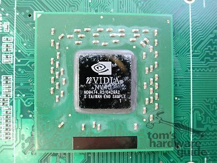
We have already covered the architecture of the GeForce 6600 family in detail. To summarize, NVIDIA has basically taken the design of the GeForce 6800, code named NV40, and taken the axe to the pixel (3) and vertex (8) pipelines to cut down on transistors and, consequently, production costs. Beyond that, the memory interface was also slimmed down from 256 bits to 128 bits. The result is a transistor count of 146 million transistors.
The chip is manufactured using a 0.11µm process. NVIDIA will be offering two versions of the card. These are the faster GeForce 6600 GT, which features GDDR 3 memory, SLI capability and clock speeds of 500 MHz (core) and 1000 MHz (DDR memory speed). Aside from sporting ordinary DDR1 memory, the vanilla GeForce 6600 will only differ from the GT in that it lacks the SLI capability and runs at lower clock speeds (300 MHz core, around 550 MHz memory). Both chips are native PCI Express parts. The AGP versions of the GeForce 6600 cards, to be launched at a later date, will therefore employ NVIDIA's HSI chip. Read what this smart little bridge chip does at Future Promise for Graphics: PCI Express .
Of course, all of this has been general knowledge for some weeks now. So now that we've covered the necessary theoretical background, let's see how NVIDIA's new mainstream card performs in practice.
Get Tom's Hardware's best news and in-depth reviews, straight to your inbox.
Current page: Introducing The GeForce 6600
Prev Page NVIDIA GeForce 6600 GT Performance Evaluation Next Page Test Setup