How to Overclock RAM
Get Tom's Hardware's best news and in-depth reviews, straight to your inbox.
You are now subscribed
Your newsletter sign-up was successful
Background
When most people talk about RAM overclocking, they tend to think of increased data rates, which requires boosting the memory's operating frequency. This is a multiple of the base clock rate (BCLK) and memory multiplier.
The memory multiplier (formerly called the memory divider) is the ratio between the RAM's clock speed and the BCLK. An example would be a 1:4 value for this ratio via a 200 MHz BCLK and 1600 MT/s DDR3 RAM (note that DDR3 RAM is double-rate, so that a 1600 MT/s data rate occurs at an 800 MHz clock rate).
Because “RAM speed” = BCLK x Multiplier, increasing the BCLK to overclock the processor increases the memory frequency automatically. But in addition to the base clock rate, a number of other parameters (often inter-related) affect memory performance and stability—operating voltages, latencies, channel/rank configurations, etc., and the task of optimizing all of these variables comes under the umbrella of memory “overclocking.”
Article continues belowBefore we get into the details of this, we need to go over some memory-specific jargon, memory classifications, and what exactly each overclocking parameter represents.
Memory Naming And Classification
There is a wide variety of system RAM, including standard SDRAM, EDO SDRAM, RDRAM, and DDR SDRAM. Today we'll focus on the DDR3 and DDR4 variety.
DRAM is most commonly identified by four numbers in addition to its manufacturer and type (DDR, DDR2, DDR3, DDR4): the total memory capacity (8GB, for example), the data rate (say, 1333 MT/s), its bandwidth (e.g. 3200 MB/s), and its timing classification (7-7-7-21 is one such configuration).
DRAM (Dynamic Random Access Memory) is an integrated circuit (IC) with a two-dimensional grid of memory cells; each cell represents a bit, with the columns called bitlines and rows called wordlines, and the row/column number of a cell represents its memory address. The number of cells determines the DRAM chip's total capacity.
Get Tom's Hardware's best news and in-depth reviews, straight to your inbox.
Physically, a memory cell is made up of a transistor-capacitor pair: the capacitor stores electric charge (a “0” if the charge is less than 50%, “1” if the charge is greater) and the transistor acts as a switch to couple charge in and out of the capacitor. But a capacitor does not stay charged for long; the charge leaks, and needs to be refreshed. This refresh cycle is what makes RAM dynamic. A memory controller (integrated into the CPU in many modern systems) reads the data, then writes it back. The frequency of the oscillator that controls these charge/discharge (read/write) cycles is the RAM's clock frequency, measured in number of cycles per second (usually MHz).
The clock rate shouldn't be confused with the speed at which information is read and written. The data rate, measured in millions of transfers per second (MT/s) determines this. Each generation of memory technology (DDR, DDR2, DDR3, DDR4) improves the maximum frequency capability, bandwidth, latency, and power usage of the chips. Double data rate RAM communicates twice per cycle, so with a clock speed of, say, 600 MHz, DDR RAM would yield 600 MHz x 8 bytes x 2 for a peak throughput of 9600 MB/s.
There is a bit of ambiguity when it comes to memory technology naming. For example, DDR3-1333 does not have a clock frequency of 1333 MHz, but half that.
The final differentiator between RAM chips is the timing classification, which represents how many clock cycles of delay there are between certain events. So, if an imaginary chip (that dispenses with architectural and basic physics limits) had a timing classification of 1-1-1-1, it would mean that it is returning data and carrying out each type of internal task once per clock cycle. The take-away: aim for the lowest possible numbers in the timing classification.
Memory Type And Configuration: DDR3 vs. DDR4
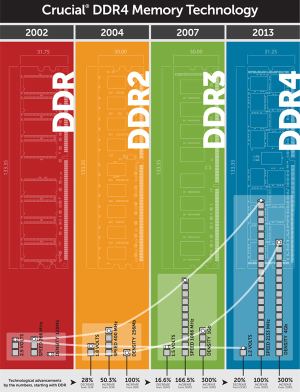
Differences in the core specifications of DDR3 and DDR4 RAM are of critical interest to overclockers. Overall, each subsequent generation of RAM brings improvements, and in this case the improvement from DDR3 to DDR4 confers lower power consumption, lower latency, and a far greater range of frequencies.
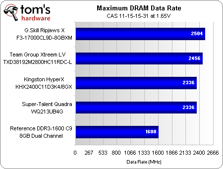
In terms of data rate, the maximum for a standard DDR3 RAM module (“standard” as defined by the Joint Electron Device Engineering Council, an independent semiconductor standards body) is 2133 MT/s, though various high-end chips surpass this limit quite easily. DDR4 does have a maximum as well, but it hasn’t been reached yet—every so often, RAM vendors crack the ceiling of data rates DDR4 RAM is capable of, and rates of more than 3000 MT/s are now sold off-the-shelf.
DDR4 is also more power-friendly than DDR3, which employs a default voltage of 1.5V. Many overclocked setups show voltages in the 1.65 to 2.0V region, while DDR4 generally has an operating voltage of 1.2V with higher bandwidth. Overclocked DDR4 kits reportedly use anywhere between 1.4 and 1.8V. Having the same or higher data rate at lower voltages means less chance of permanent damage, lower cooling requirements, and more headroom for overclocking—all good things.
There are other core differences between DDR3 and DDR4, including maximum capacity, but these are peripheral for overclocking purposes. And this is obvious but bears mention: an overclocker using a previous-gen CPU cannot use DDR4 RAM—Intel’s Skylake design is the best bet when it comes to CPU/IMC compatibility.
Channel, Rank, and Side
Single- versus multi-channel, when it comes to memory, is a CPU-side mode. The IMC can use multiple parallel channels to access the memory, theoretically doubling the bandwidth, though real-world gains are typically less than ideal. The high-end CPUs used by overclockers now feature up to four-channel architectures, but the motherboard must support this.
A memory rank is a lower-level grouping of individual memory chips on a single memory module—a data block that is 64 bits wide. Single rank means that all the memory modules belong to one addressable block; dual rank means that the memory modules on a chip are divided into two groups. Rank does not depend on the number of physical memory chips on a memory module.
Depending on the CPU/IMC configuration, the maximum number of ranks supported per channel is limited; there are performance gains to be had by increasing the number of ranks in a configuration, but too many ranks negatively impact overall memory speed (though in general this will only come into play for servers, workstations, and other high memory-capacity configurations).
Single- versus double-sided RAM is a question of density. Single-sided memory sticks have all of the memory ICs in a high-density configuration on only one side of the physical module, whereas double-sided RAM has the packages on both sides. The two types can be one-, two-, three-, or four-rank. There is a lot of controversy regarding performance of single-/double-sided RAM, mostly because high-frequency, high-density, single-sided RAM is also often single-rank, and shows a noticeable reduction in benchmark scores compared to lower-clocked, double-sided, dual-rank RAM.
Interleaving is the process of dividing data blocks such that multiple targets can be addressed contiguously. Channel interleaving increases the potential read bandwidth of the system, and rank interleaving means one rank of memory can be addressed while another is being refreshed (for multi-rank configurations), reducing the chip's overall latency. Channel and rank interleaving parameters should be set to the highest possible supported by the motherboard to maximize memory performance.
Primary RAM Timings
A memory module’s timings are shown as a set of four numbers, for example 7-8-7-24. Each of these numbers stands for timing delay associated with an internal task type (identified by one of the acronyms defined below), and the order of the numbers is always CL-tRCD-tRP-tRAS.
In order to read or write data to a specific memory address (cell), first the row pertaining to that cell has to be activated, then the column. Each activation process is a separate task, and has various timings (or delays, in clock cycles) associated with it.
CL, the CAS Latency, which stands for Column Address Strobe Latency. It refers to the delay between sending a column address to the memory controller and receiving a result. This is arguably the parameter with the largest impact on RAM latency and performance.
tRCD, also known as RAS to CAS delay, where RAS stands for Row Address Strobe. This is the number of clock cycles it takes to activate a column of data (CAS) of a previously activated row (RAS).
tRP, also known as the RAS Precharge delay, is the delay between closing off read/write access to one row of data and opening access to a different one.
tRAS, the Row Active Time, is the number of cycles required to successfully retrieve data stored in a row; it can be thought of as a wait/delay (in number of clock cycles) before a new request to access a memory cell can begin.
There is a fifth timing classification, CMD, also known as the Command Rate. This is not often reported, but it is the delay between activation of memory and receipt of commands, and is often one or two cycles. There are also secondary and tertiary groups of timings. You can further improve performance by optimizing them, though the gains aren't as significant as what you get from the primary timings.
The timings listed above do depend on each other. For example, the amount of time it takes to access a new memory cell (after accessing a previous one) is tRAS (for a successful retrieval of data in the previous cell) + tRP (to switch to a different row) + tRCD (delay to access a column) + tCL (result from the cell itself). Also, the tRAS time is pre-configured to be greater than the sum of tCL, tRCD, tRP, though overclockers have posted benchmark configurations that defy this rule.
Voltages That Affect Memory
We covered a number of voltages in our processor overclocking article, but some processor-side and motherboard-side voltages are also relevant to memory overclocking. CPUs from both Intel and AMD have integrated memory controllers, and not all of the following voltages will be relevant for all chipsets/processor generations.
Obviously, the most important voltage with respect to memory is the memory voltage, called a variety of names depending on the motherboard firmware and chipset, including VDDQ, SSTL (Stub Series Termination Logic) voltage, DIMM Voltage, DRAM Voltage, VDIMM Select, etc. This value is set to 1.5V (usually) for DDR3 and 1.2V for DDR4 as a default.
The VTT (termination voltage) goes by many names. It can be found listed as IMC Voltage or QPI/VTT Voltage and others, but it is the voltage fed to the IMC on-board the CPU. There are differences between Intel pre-Sandy Bridge, Intel post-Sandy Bridge, and AMD terminology here: modern Intel processors call this the VCCSA (also called “system agent”), and AMD calls this the VDDNB. This is the voltage that can be tweaked if changes in BCLK introduce instabilities.
The Reference Voltage, also called the VREFDQ, DRAM Ctrl Ref Voltage, DDR_VREF_CA_A, etc., sets the threshold for a voltage level to be considered a “0” or a “1.”
The VDDNB is the voltage supplied to the IMC, but the “NB” part refers to northbridge, and other memory options may look very similar; it is best to look up the chipset and motherboard specific definition of this term before changing the values.
The DRAM voltage and perhaps the voltage supplied to the IMC (whatever the variable is named in a specific system motherboard/processor configuration) are the only values that need to be touched in the beginning stages of memory overclocking.
-
Sakkura Perfect timing, I was just about to get to work on my DDR3-1600 kit. Gotta squeeze out all the performance possible from my aging Ivy Bridge build. Especially now that I'm running VR.Reply -
BobsKnob You know why there's no benchmarks? Because overclocking memory offers such small 'real world' gains that it's not even worth it. You might as well try to overclock your usb ports. This is just a lame attempt to advertise products, in this case Kingston and Arctic heat spreaders and try to pass it off as reporting.Reply -
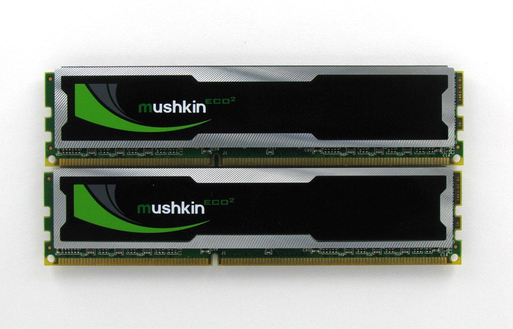
derekullo They also mentioned Mushkin, Crucial and G.Skill.Reply
Heaven forbid they mention the manufacturer of the ram in an article about overclocking ram.
Now if this would have been an article about Farcry 5 or Elder Scrolls 6 and they had a picture of an Arctic Heat Spreader then you would have been on to something. -
BobsKnob Thank you for proving my point. It's just advertising masquerading as reporting.Reply
You know, there used to be a time when Tom's did real, unbiased reviews and reporting. When something sucked...it sucked and the review wasn't candy coated. -
dish_moose I'm with Bob on this one - until you show real wold benchmarks showing real improvement from OC RAM, I won't waste my time.Reply
-Bruce -
Maxxtraxx Check out the youtube channel Digital Foundry, this video specifically: https://www.youtube.com/watch?v=Er_Fuz54U0YReply -
Maxxtraxx Proof of increased performance from Ram Overclocking from real world benchmarks can be found here:Reply
https://www.youtube.com/watch?v=Er_Fuz54U0Y
Am I not allowed to edit my own posts? or am i really missing something here? I wanted to say more after I posted but could not find any way to edit my own post.
