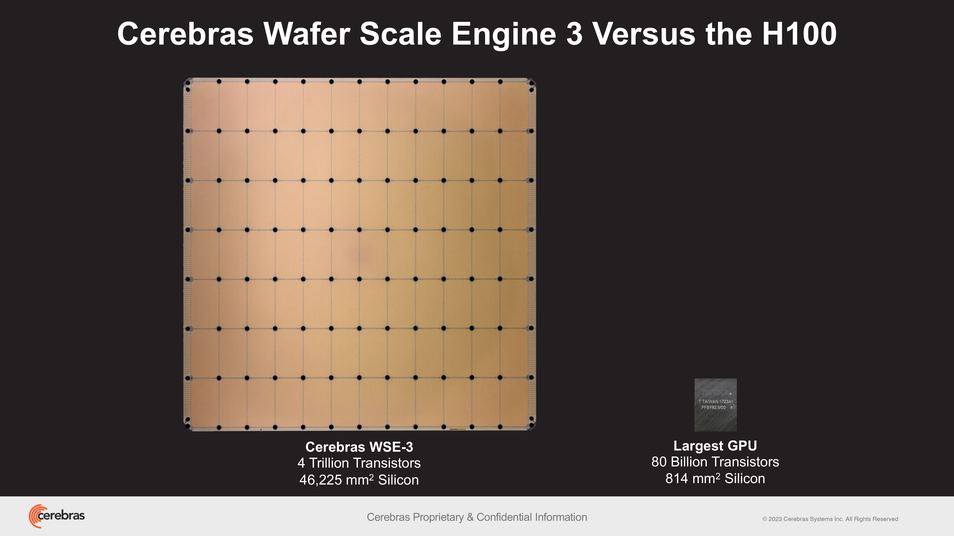
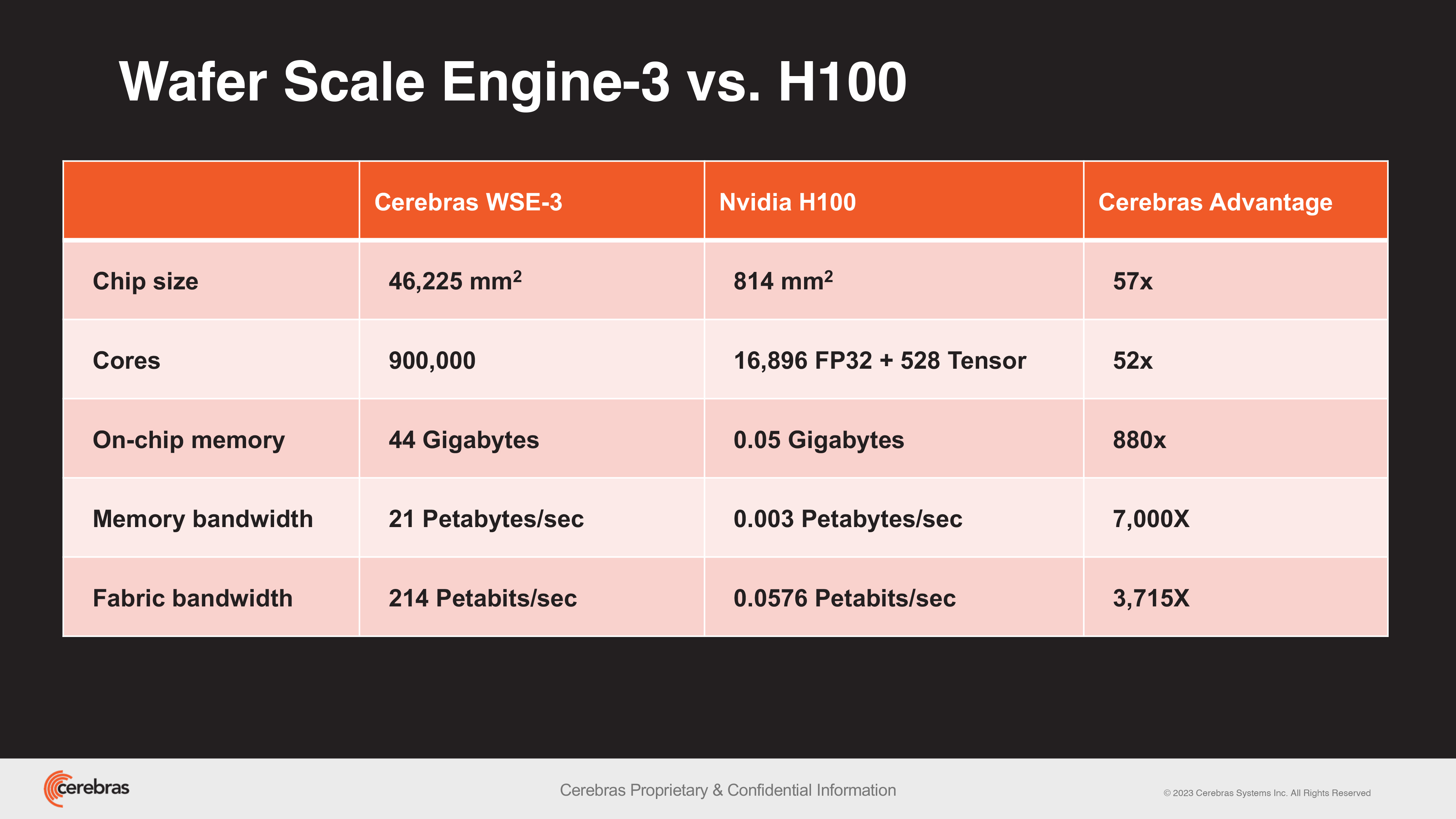
Cerebras launches 900,000-core 125 PetaFLOPS wafer-scale processor for AI — theoretically equivalent to about 62 Nvidia H100 GPUs
Cerebras launches WSE-3 wafer-scale processor, CS-3 supercomputer.
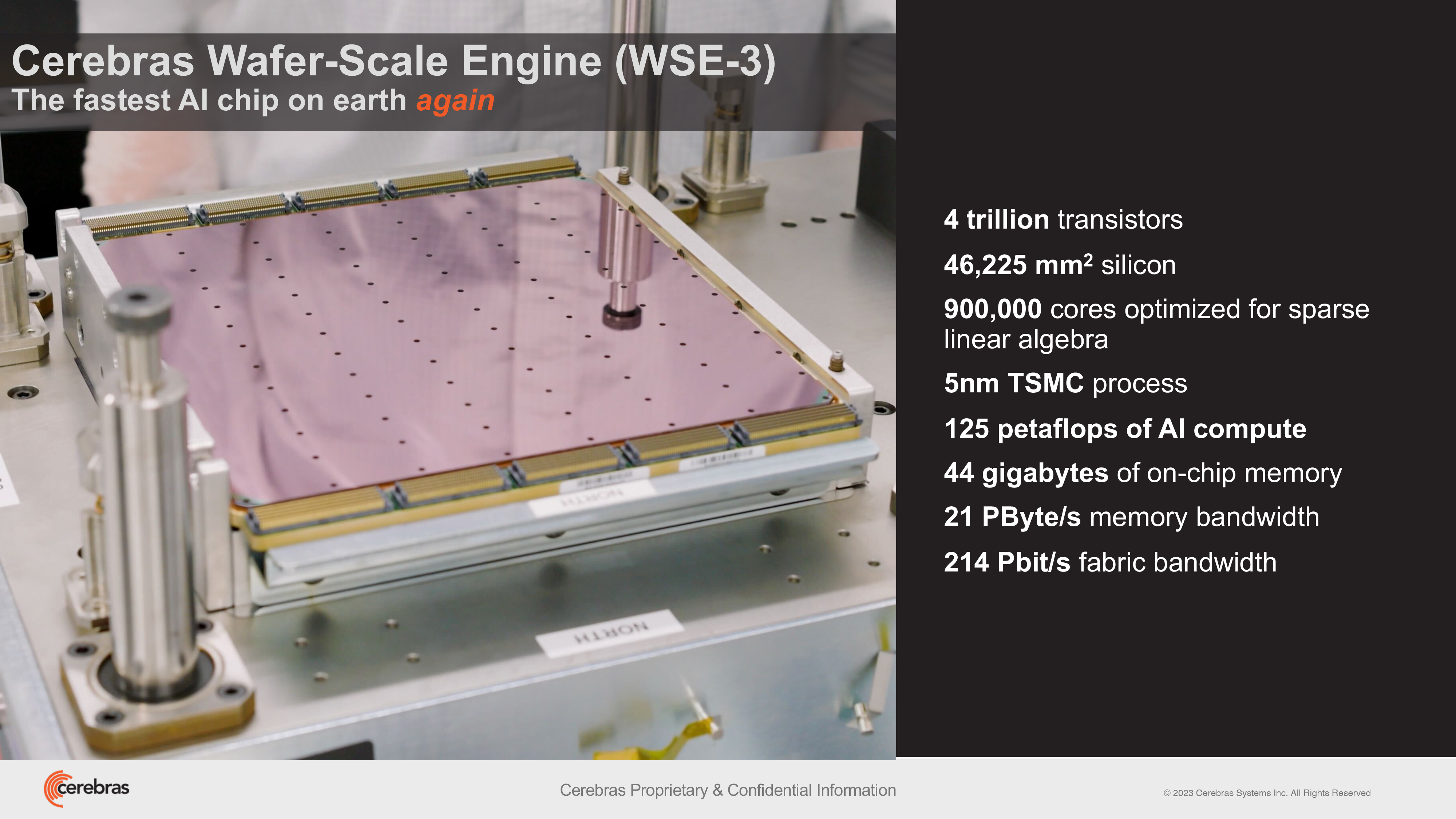
Cerebras Systems has unveiled its Wafer Scale Engine 3 (WSE-3), a breakthrough AI wafer-scale chip with double the performance of its predecessor, the WSE-2. This new device packs 4 trillion transistors made on TSMS's 5nm-class fabrication process; 900,000 AI cores; 44GB of on-chip SRAM; and has a peak performance of 125 FP16 PetaFLOPS. Ceberas's WSE-3 will be used to train some of the industry's largest AI models.
The WSE-3 powers Cerebras's CS-3 supercomputer, which can be used to train AI models with up to 24 trillion parameters — a significant leap over supercomputers powered by the WSE-2 and other modern AI processors. The supercomputer can support 1.5TB, 12TB, or 1.2PB of external memory, which allows it to store massive models in a single logical space without partitioning or refactoring — streamlining the training process and enhancing developer efficiency.
In terms of scalability, the CS-3 can be configured in clusters of up to 2048 systems. This scalability allows it to fine-tune 70 billion parameter models in just one day with a four-system setup, and to train a Llama 70B model from scratch in the same timeframe at full scale.
The latest Cerebras Software Framework offers native support for PyTorch 2.0 and also supports dynamic and unstructured sparsity, which can accelerate training — up to eight times faster than traditional methods.
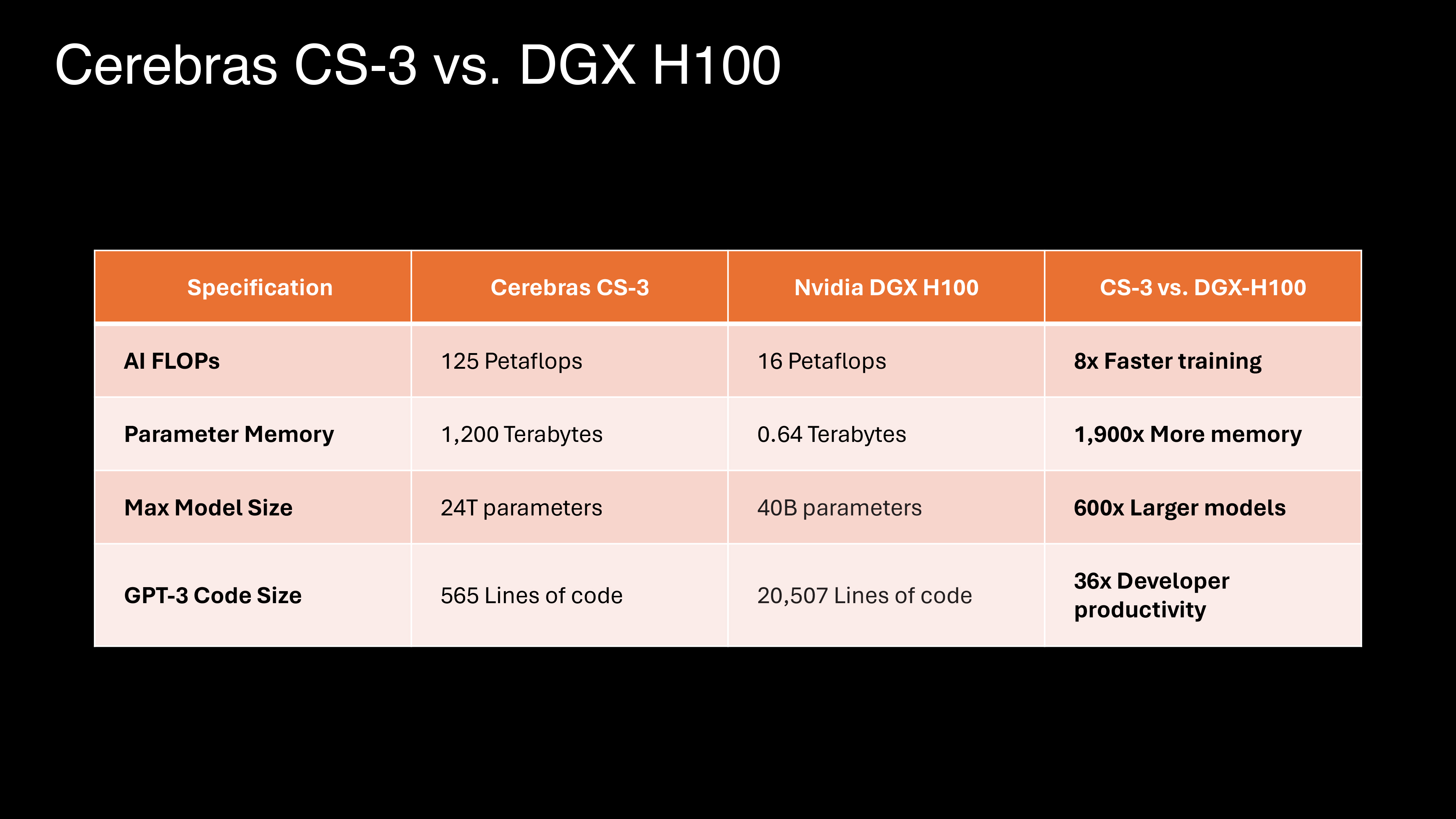
Cerebras has emphasized the CS-3's superior power efficiency and ease of use. Despite doubling its performance, the CS-3 maintains the same power consumption as its predecessor. It also simplifies the training of large language models (LLMs), requiring up to 97% less code compared to GPUs. For example, a GPT-3 sized model requires only 565 lines of code on the Cerebras platform, according to the company.
The company has already seen significant interest in the CS-3, and has a substantial backlog of orders from various sectors — including enterprise, government, and international clouds. Cerebras is also collaborating with institutions such as the Argonne National Laboratory and the Mayo Clinic, highlighting the CS-3's potential in healthcare.
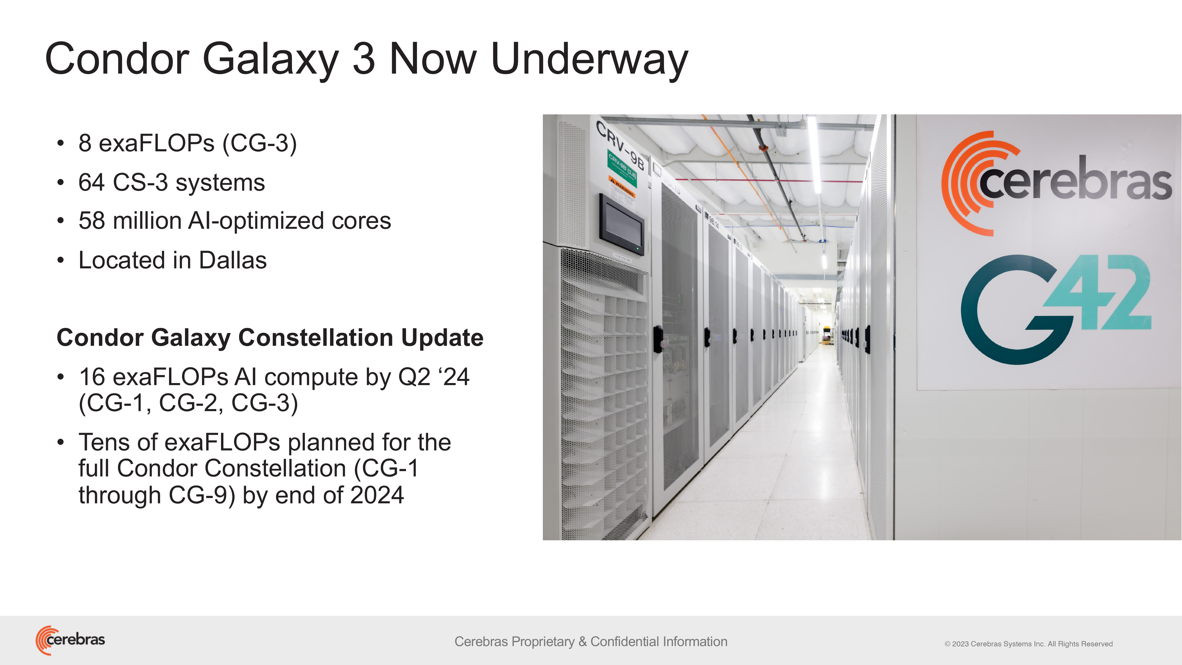
A strategic partnership between Cerebras and G42 is also set to expand with the construction of the Condor Galaxy 3, an AI supercomputer featuring 64 CS-3 systems (packing a whopping 57,600,000 cores). Together, the two companies have already created two of the biggest AI supercomputers in the world: the Condor Galaxy 1 (CG-1) and the Condor Galaxy 2 (CG-2), which are based in California and have a combined performance of 8 ExaFLOPs. This partnership aims to deliver tens of exaFLOPs of AI compute, globally.
Get Tom's Hardware's best news and in-depth reviews, straight to your inbox.
"Our strategic partnership with Cerebras has been instrumental in propelling innovation at G42, and will contribute to the acceleration of the AI revolution on a global scale," said Kiril Evtimov, Group CTO of G42. "Condor Galaxy 3, our next AI supercomputer boasting 8 exaFLOPs, is currently under construction and will soon bring our system’s total production of AI compute to 16 exaFLOPs."

Anton Shilov is a contributing writer at Tom’s Hardware. Over the past couple of decades, he has covered everything from CPUs and GPUs to supercomputers and from modern process technologies and latest fab tools to high-tech industry trends.
-
gg83 So cerebras is better per transitor. If one cerebras has 4 trillion transistors and it's "equivalent" to 62 H100's @ 80 billion transistors each, I get 4 trillion to 4.96 trillion on the nvidia side. Maybe my math is nonsense. If Cerebras can pull this off, could tenstorrent have a harder time getting in to the top AI game?Reply -
vanadiel007 1 million trillion billion and a few spares coming in next.Reply
Just counting the 4 trillion transistors would likely take a lifetime... -
Amdlova One chip to rule all.Reply
54gb on chip memory It's have more cache than I have memory on my computer. -
ivan_vy Reply
maybe if you add your two systems. :)Amdlova said:One chip to rule all.
54gb on chip memory It's have more cache than I have memory on my computer. -
bit_user Chips like this are why Sam Altman wants to scale up global fab capacity by like 10x.Reply
I'm a little curious why none of their slides (at least of those shown here) highlighted energy efficiency. I expect that's also an area of considerable lead over Nvidia. I'd be even more curious to know how perf/$ compares! -
bit_user Reply
Technically one chip, but the tiles are effectively different chips.Amdlova said:One chip to rule all.
Accessing SRAM from another tile probably takes longer than your CPU does to read any part of your DRAM. That's not to say one is better or worse than the other, in the abstract.Amdlova said:54gb on chip memory It's have more cache than I have memory on my computer.
Their solution is very much suited towards dataflow processing and is nearly ideal, if you can fit all of your weights in the 44 GB* on a single wafer. Also, you want those weights to roughly align with the computational density of the network. Otherwise, there could be some underutilization of either compute or memory.
* Image indicates 44 GB of SRAM. -
JTWrenn Wait....only 8 times faster on the AI FLOPs? 50 times the transistors and only 8 times the compute? How are they going to deal with chip manufacturing issues at that level to get manufacturing up? It's an interesting idea but....this just seems like a weird approach.Reply
Will be glad to see some real competition for Nvidia but this idea seems like it may have a lot of issues. Maybe I am missing something. -
bit_user Reply
You're getting mixed up between system specifications and chip specifications. A "DGX H100" system contains 8x H100 chips.JTWrenn said:Wait....only 8 times faster on the AI FLOPs? 50 times the transistors and only 8 times the compute? How are they going to deal with chip manufacturing issues at that level to get manufacturing up? It's an interesting idea but....this just seems like a weird approach.
Compute-wise, it's worth pointing out that Nvidia touts the DGX H100's 32 TFLOPS of fp8 performance, which is probably why Cerebras is focusing on training performance. On that front (BF16), the DGX H100 has only 16 TFLOPS.
References:
https://docs.nvidia.com/dgx/dgxh100-user-guide/introduction-to-dgxh100.html https://nvidianews.nvidia.com/news/nvidia-announces-dgx-h100-systems-worlds-most-advanced-enterprise-ai-infrastructure -
nightbird321 Reply
I'm going to go with 44GB since that is what is in the article.Amdlova said:One chip to rule all.
54gb on chip memory It's have more cache than I have memory on my computer.
44GB over 900,000 cores is only 50KB per core of cache memory which is tiny compared with consumer CPUs. As a specific purpose chip with specifically written code, it likely doesn't need a big memory for random access. (Unless I am misunderstanding what they mean by on-chip memory) -
bit_user Reply
If you compute the amount of silicon area or transistors per core, it's pretty clear that these are probably similar to what Nvidia calls a "core". In other words, something more like a SIMD lane.nightbird321 said:44GB over 900,000 cores is only 50KB per core
I doubt it works as cache, but is probably directly addressable. Cache lookups require associative memory, which wastes die space and power for something that's really not necessary, when your access patterns are predictable. The normal way this works is you have a double-buffering type scheme and you've got a DMA engine which drains/fills inactive buffers while you're computing on the contents of the active buffer.nightbird321 said:of cache memory which is tiny compared with consumer CPUs.
The IBM Cell processor worked this way, which was popularly used in Sony's PS3. Each of its 8 SPEs had 256 kB of SRAM that it used like this. The SPEs had no direct access to system memory, but rather relied upon DMAs to copy everything in/out of their scratchpad memory.
https://en.wikipedia.org/wiki/Cell_(processor)#Overview
I think a big use case for external DRAM access is streaming in weights, in the event you don't have enough SRAM to keep them all on-die. That's probably what eats most of the massive memory bandwidth on Nvidia's Hopper, for instance.nightbird321 said:As a specific purpose chip with specifically written code, it likely doesn't need a big memory for random access. (Unless I am misunderstanding what they mean by on-chip memory)
