PCIe 6.0 Spec at Final Draft: 128 GBps
PCIe Gen6 at 64 GT/s with PAM4 encoding is nearly here.

PCI-SIG this week announced that the PCIe 6.0 specification has reached its Final Draft status, which is an important milestone that formally marks completion of the development. All system-on-chips compliant with the PCIe 6.0 version 0.9 specification will be compliant with the final 1.0 version of the technology. The only question is which applications will actually need to adopt PCIe Gen6.
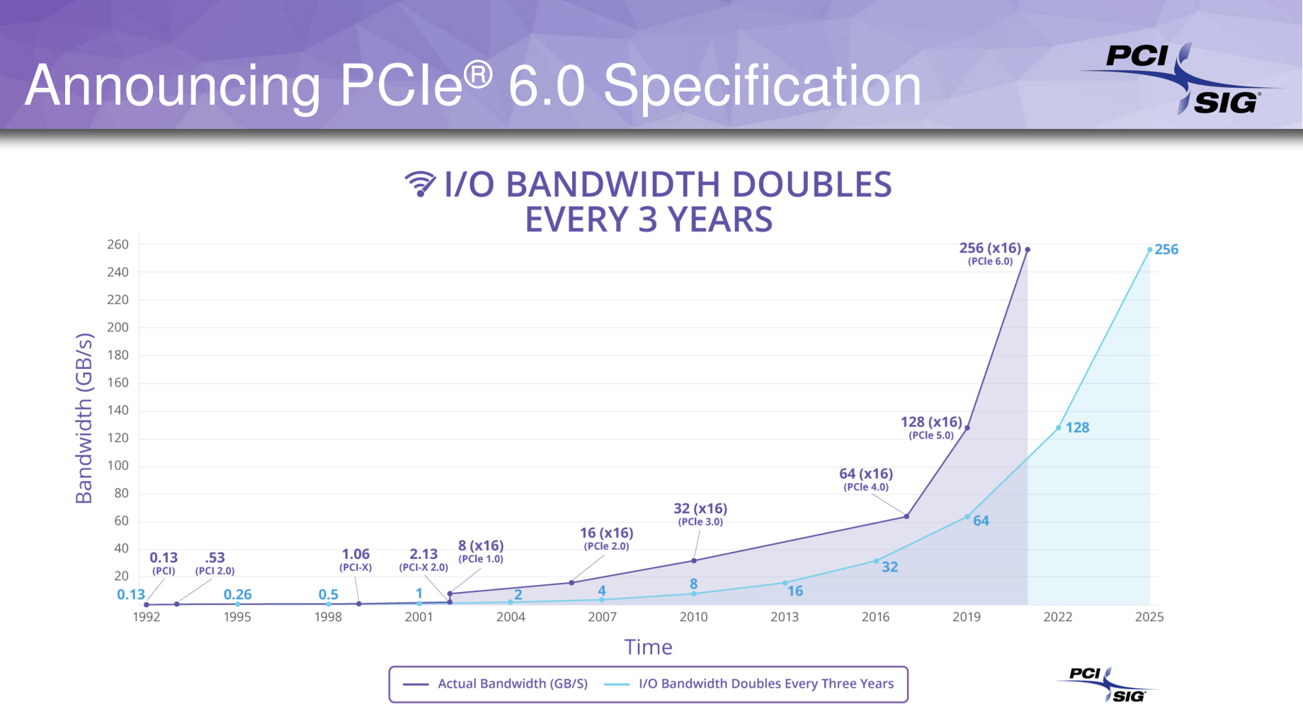
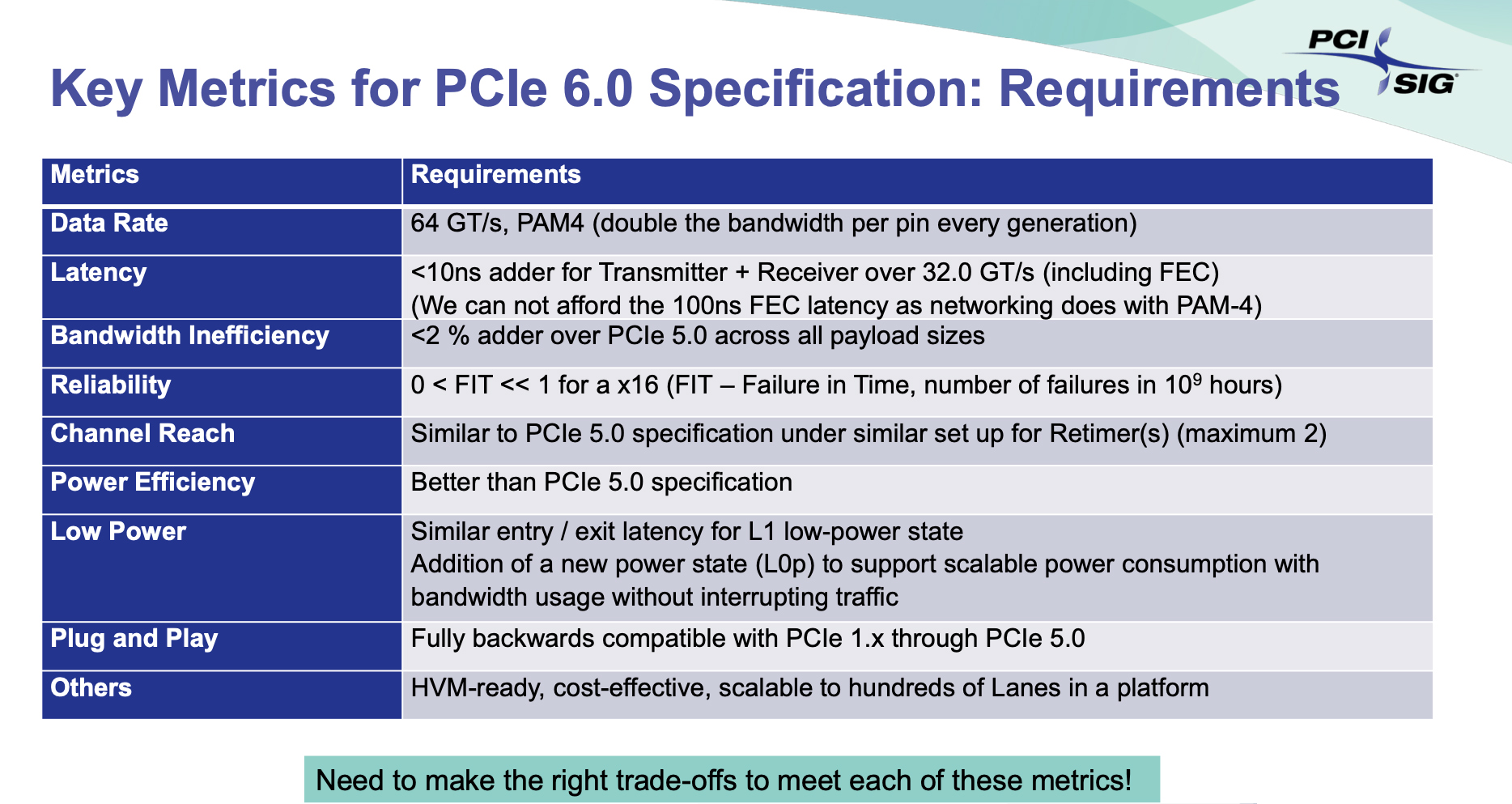
PCIe Gen6 will boost data transfer rate to 64 GT/s per pin, up from PCIe Gen5's 32 GT/s and PCIe Gen4's 16 GT/s, but will maintain backwards compatibility with existing hardware. The new technology allows data transfer of up to 128 GB per second in each direction over an x16 interface.
PCI Express specifications have five primary checkpoints: Concept, First Draft, Complete Draft, Final Draft, and Final. The release of PCIe 6.0 Complete Draft (version 0.7) spec a little less than a year ago enabled big companies as well as technology developers like Synopsys to start implementing their PCIe 6.0 controller IP and PHY in silicon. The publication of the PCIe 6.0 Final Draft (version 0.9) specification marks a point after which no functional changes are permitted and members of PCI-SIG should start reviewing the standard for their intellectual property and patents.
Those companies who have managed to incorporate PCIe 6.0 v0.9 support into their system-on-chips (SoCs) theoretically can start selling them as 'PCIe 6.0 Ready', yet they will be unable to formally confirm compliancy with the final PCIe 6.0 version 1.0 specifications since there is no formal PCIe 6.0 compliance program right now and no PCIe 6.0 compliance workshops take place.
To make such extreme data transfer rates and bandwidth possible, developers of the new standard have to adopt pulse amplitude modulation with four levels (PAM-4) of signaling, which is also used for high-end networking technologies like InfiniBand as well as GDDR6X memory. Also, PCIe Gen6 features low-latency forward error correction (FEC) to ensure high efficiency at high data rates.
While PCIe 6.0 is a major step forward for the interface as it brings in numerous innovations and dramatically increases performance, it will also present numerous challenges to chip and system designers. First up, PAM-4 is always expensive in terms of power and in terms of die size, which is why it has not been adopted widely beyond 100GbE and 200GbE high-end datacenter or enterprise-grade networking standards. Secondly, 64 GT/s is a very high data transfer rate and while PAM-4 with FEC will help to mitigate some of the difficulties, signal transmission over the printed circuit boards (PCBs) will have to be optimized for crosstalk, loss, reflections, and power integrity.
Essentially, this means that not all SoC designers (especially in the client PC space) will be eager to adopt PCIe 6.0 due to cost and power concerns. Furthermore, implementing PCIe 6.0 on the system level will require complex PCBs and frequent usage of expensive retimers and redrivers over relatively short distances. All-in-all, while PCIe 6.0 makes a lot of sense for servers and specialized systems, it may be too expensive for wide usage in client PCs, so consumer-grade GPUs and SSD controllers may adopt it.
Get Tom's Hardware's best news and in-depth reviews, straight to your inbox.

Anton Shilov is a contributing writer at Tom’s Hardware. Over the past couple of decades, he has covered everything from CPUs and GPUs to supercomputers and from modern process technologies and latest fab tools to high-tech industry trends.

