Socket 370: April 1998 To July 2001
| Intel Celeron 233 to 533 | April 1998 to January 2000 |
| Pentium III/500 to 1133 | October 1999 to July 2001 |
| Celeron II/533 to 1100 | January 2000 to July 2001 |
| Celeron/Pentium III/1000 to 1400 | January 2000 to July 2001 |
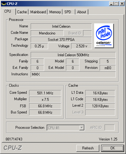
There were many users who left out Slot 1 as a processor platform for reasons of cost. Because as early as 1998 the next development was ready: Socket 370, for which there were two case variations - the PPGA and the FC-PGA. The PPGA was predominantly used in OEM systems because it was cheaper to manufacture. In the aforementioned, only the Celeron was used in the plastic package; the Pentium III CPUs came in the more expensive FC-PGA package. And there was one exception: The Celeron with Mendocino core could be used in both sockets. But there was also help: using an adapter, the PPGA CPUs could also be used in Slot 1; for the FC-PGA version there was no adapter.

Adapter of Slot 1 on Socket 370. The settings for the voltage and bus speed had to be defined manually.
For a long time, the CPUs for Slot 1 and Socket 370 were being made and sold simultaneously, although the Pentium III (Coppermine) from 1 GHz clock speed and up met its end in Slot 1.
The last core for Socket 370 was the Tualatin, which meant a transformation (shrink) from 180 nm to 130 nm. The Pentium III-S was made with up to 1.4 GHz and a 512 kB L2 cache. Moreover, this core had data prefetch expansions, which were the forerunner of the micro-ops of today's Pentium 4.

The last Socket 370 CPU, the Pentium III-S Tualatin with 1.4 GHz
