Nvidia’s Turing Architecture Explored: Inside the GeForce RTX 2080
Get Tom's Hardware's best news and in-depth reviews, straight to your inbox.
You are now subscribed
Your newsletter sign-up was successful
Turing Improves Performance in Today’s Games
Some enthusiasts have expressed concern that Turing-based cards don’t boast dramatically higher CUDA core counts than their previous-gen equivalents. The older boards even have higher GPU Boost frequencies. Nvidia didn’t help matters by failing to address generational improvements in today’s games at its launch event in Cologne, Germany. But the company did put a lot of effort into rearchitecting Turing for better per-core performance.
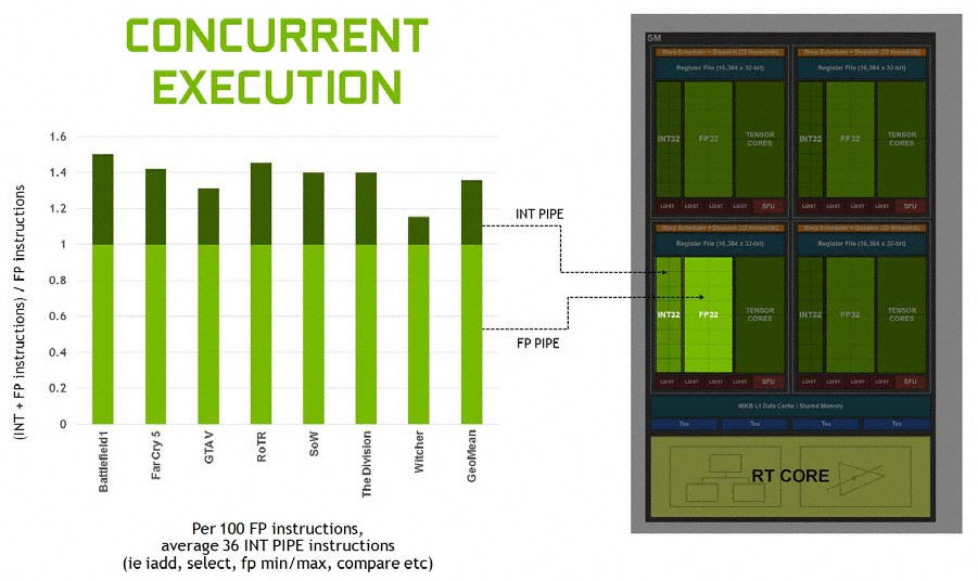
To start, Turing borrows from the Volta playbook in its support for simultaneous execution of FP32 arithmetic instructions, which constitute most shader workloads, and INT32 operations (for addressing/fetching data, floating-point min/max, compare, etc.). When you hear about Turing cores achieving better performance than Pascal at a given clock rate, this capability largely explains why.
In generations prior, a single math data path meant that dissimilar instruction types couldn’t execute at the same time, causing the floating-point pipeline to sit idle whenever non-FP operations were needed in a shader program. Volta sought to change this by creating separate pipelines. Although Nvidia eliminated the second dispatch unit assigned to each warp scheduler, it also claimed that instruction issue throughput rose.
Article continues belowHow is that possible? It's all about the composition of each architecture's SM.
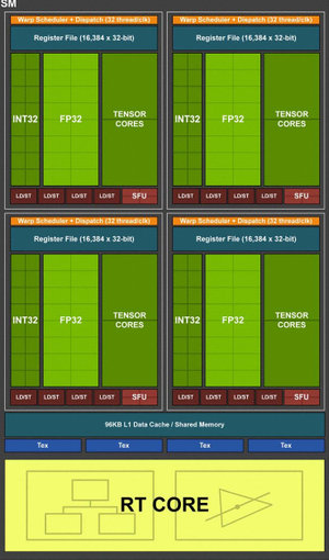
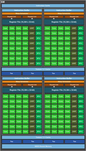
Check out the two block diagrams below. Pascal has one warp scheduler per quad, with each quad containing 32 CUDA cores. A quad's scheduler can issue one instruction pair per clock through the two dispatch units with the stipulation that both instructions come from the same 32-thread warp, and only one can be a core math instruction. Still, that's one dispatch unit per 16 CUDA cores.
In contrast, Turing packs fewer CUDA cores into an SM, and then spreads more SMs across each GPU. There's now one scheduler per 16 CUDA cores (2x Pascal), along with one dispatch unit per 16 CUDA cores (same as Pascal). Gone is the instruction-pairing constraint. And because Turing doubles up on schedulers, it only needs to issue an instruction to the CUDA cores every other cycle to keep them full (with 32 threads per warp, 16 CUDA cores take two cycles to consume them all). In between, it's free to issue a different instruction to any other unit, including the new INT32 pipeline. The new instruction can also be from any warp.
Turing's flexibility comes from having twice as many schedulers as Pascal, so that each one has less math to feed per cycle, not from a more complicated design. The schedulers still issue one instruction per clock cycle. It's just that the architecture is better able to utilize resources thanks to its improved balance throughout the SM.
Get Tom's Hardware's best news and in-depth reviews, straight to your inbox.
According to Nvidia, the potential gains are significant. In a game like Battlefield 1, for every 100 floating-point instructions, there are 50 non-FP instructions in the shader code. Other titles bias more heavily toward floating-point math. But the company claims there are an average of 36 integer pipeline instructions that would stall the floating-point pipeline for every 100 FP instructions. Those now get offloaded to the INT32 cores.
Despite the separation of FP32 and INT32 paths on its block diagrams, Nvidia says each Turing SM contains 64 CUDA cores to keep things straightforward. The Turing SM also comprises 16 load/store units, 16 special-function units, 256KB of register file space, 96KB of shared memory and L1 data cache, four texture units, eight Tensor cores, and one RT core.
On paper, an SM in the previous-generation GP102 appears more complex, sporting twice as many CUDA cores, load/store units, SFUs, texture units, just as much register file capacity, and more cache. But remember that the new TU102 boasts as many as 72 SMs across the GPU, while GP102 topped out at 30 SMs. The result is a Turing-based flagship with 21% more CUDA cores and texture units than GeForce GTX 1080 Ti, but also way more SRAM for registers, shared memory, and L1 cache (not to mention 6MB of L2 cache, doubling GP102’s 3MB).
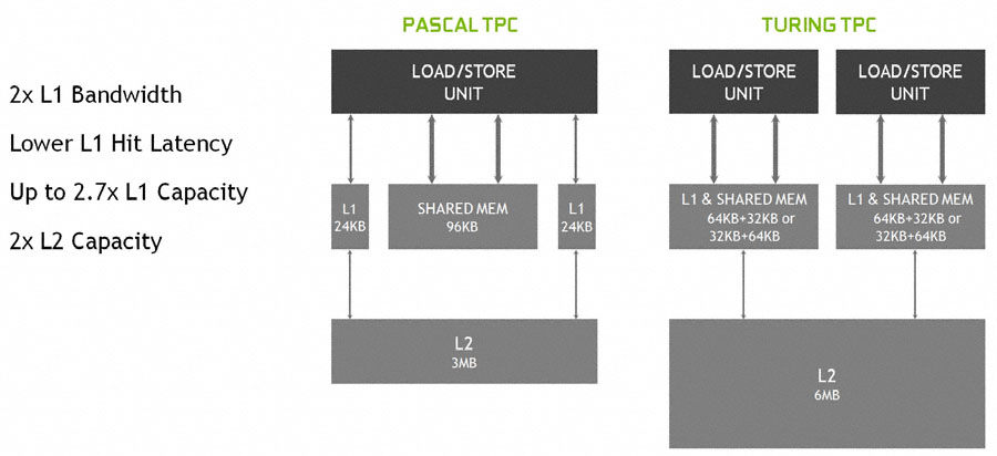
That increase of on-die memory plays another critical role in improving performance, as does its hierarchical organization. Consider the three different data memories: texture cache for textures, L1 cache for load/store data, and shared memory for compute workloads. As far back as Kepler, each SM had 48KB of read-only texture cache, plus a 64KB shared memory/L1 cache. In Maxwell/Pascal, the L1 and texture caches were combined, leaving 96KB of shared memory on its own. Now, Turing combines all three into one shared and configurable 96KB pool.
The benefit of unification, of course, is that regardless of whether a workload is optimized for L1 or shared memory, on-chip storage is utilized rather than sitting idle as it may have before. Moving L1 functionality down has the additional benefit of putting it on a wider bus, doubling L1 cache bandwidth (at the TPC level, Pascal supports 64 bytes per clock cache hit bandwidth, while Turing can do 128 bytes per clock). And because those 96KB can be configured as 64KB L1 and 32KB shared memory (or vice versa), L1 capacity can be 50% higher on a per-SM basis.
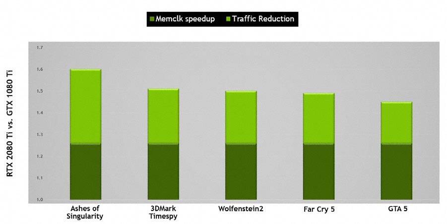
Combined, Nvidia claims that the effect of its redesigned math pipelines and memory architecture is a 50% performance uplift per CUDA core. To keep those data-hungry cores fed more effectively, Nvidia paired TU102 with GDDR6 memory and further optimized its traffic reduction technologies (like delta color compression). Pitting GeForce GTX 1080 Ti’s 11 Gb/s GDDR5X modules against RTX 2080 Ti’s 14 Gb/s GDDR6 memory, both on an aggregate 352-bit bus, you’re looking at a 27%-higher data rate/peak bandwidth figure across the board. Then, depending on the game, when RTX 2080 Ti can avoid sending data over the bus, effective throughput increases even more by double-digit percentages.
MORE: Best Graphics Cards
MORE: Desktop GPU Performance Hierarchy Table
MORE: All Graphics Content
Current page: Turing Improves Performance in Today’s Games
Prev Page Meet TU106 and GeForce RTX 2070 Next Page Designing for The Future: Tensor Cores and DLSS-
siege19 "And although veterans in the hardware field have their own opinions of what real-time ray tracing means to an immersive gaming experience, I’ve been around long enough to know that you cannot recommend hardware based only on promises of what’s to come."Reply
So wait, do I preorder or not? (kidding) -
jimmysmitty Well done article Chris. This is why I love you. Details and logical thinking based on the facts we have.Reply
Next up benchmarks. Can't wait to see if the improvements nVidia made come to fruition in performance worthy of the price. -
Lutfij Holding out with bated breath about performance metrics.Reply
Pricing seems to be off but the followup review should guide users as to it's worth! -
Krazie_Ivan i didn't expect the 2070 to be on TU106. as noted in the article, **106 has been a mid-range ($240-ish msrp) chip for a few generations... asking $500-600 for a mid-range GPU is insanity. esp since there's no way it'll have playable fps with RT "on" if the 2080ti struggles to maintain 60. DLSS is promisingly cool, but that's still not worth the MASSIVE cost increases.Reply -
jimmysmitty Reply21319910 said:i didn't expect the 2070 to be on TU106. as noted in the article, **106 has been a mid-range ($240-ish msrp) chip for a few generations... asking $500-600 for a mid-range GPU is insanity. esp since there's no way it'll have playable fps with RT "on" if the 2080ti struggles to maintain 60. DLSS is promisingly cool, but that's still not worth the MASSIVE cost increases.
It is possible that they are changing their lineup scheme. 106 might have become the low high end card and they might have something lower to replace it. This happens all the time. -
Lucky_SLS turing does seem to have the ability to pump up the fps if used right with all its features. I just hope that nvidia really made a card to power up its upcoming 4k 200hz hdr g sync monitors. wow, thats a mouthful!Reply -
anthonyinsd ooh man the jedi mind trick Nvidia played on hyperbolic gamers to get rid of thier overstock is gonna be EPIC!!! and just based on facts: 12nm gddr6 awesome new voltage regulation and to GAME only processes thats a win in my book. I mean if all you care is about is your rast score, then you should be on the hunt for a titan V, if it doesn't rast its trash lol. been 10 years since econ 101, but if you want to get rid of overstock you dont tell much about the new product till its out; then the people who thought they were smart getting the older product, now want o buy the new one too....Reply -
none12345 I see a lot of features that are seemingly designed to save compute resources and output lower image quality. With the promise that those savings will then be applied to increase image quality on the whole.Reply
I'm quite dubious about this. My worry is that some of the areas of computer graphics that need the most love, are going to get even worse. We can only hope that overall image quality goes up at the same frame rate. Rather then frame rate going up, and parts of the image getting worse.
I do not long to return to the day where different graphics cards output difference image quality at the same up front graphics settings. This was very annoying in the past. You had some cards that looked faster if you just looked at their fps numbers. But then you looked at the image quality and noticed that one was noticeably worse.
I worry that in the end we might end up in the age of blur. Where we have localized areas of shiny highly detailed objects/effects layered on top of an increasingly blurry background. -
CaptainTom I have to admit that since I have a high-refresh (non-Adaptive Sync) monitor, I am eyeing the 2080 Ti. DLSS would be nice if it was free in 1080p (and worked well), and I still don't need to worry about Gstink. But then again I have a sneaking suspicion that AMD is going to respond with 7nm Cards sooner than everyone expects, so we'll see.Reply
P.S. Guys the 650 Ti was a 106 card lol. Now a xx70 is a 106 card. Can't believe the tech press is actually ignoring the fact that Nvidia is relabeling their low-end offering as a xx70, and selling it for $600 (Halo product pricing). I swear Nvidia could get away with murder... -
mlee 2500 4nm is no longer considered a "Slight Density Improvement".Reply
Hasn't been for over a decade. It's only lumped in with 16 from a marketing standpoint becuase it's no longer the flagship lithography (7nm).
