Nvidia’s Turing Architecture Explored: Inside the GeForce RTX 2080
Meet TU102 and GeForce RTX 2080 Ti
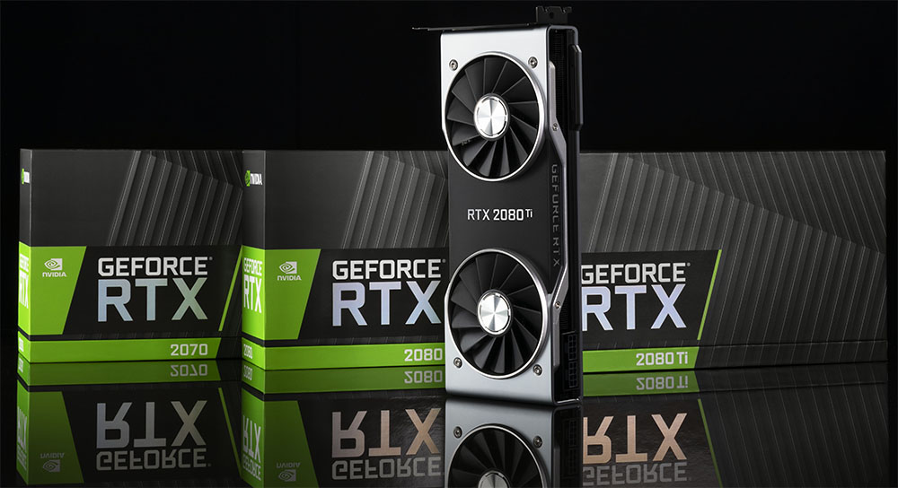
Nvidia calls Turing its biggest architectural leap forward in more than 10 years. To prove it, the company is showing off a compendium of forward-looking capabilities that speed up performance in today’s games, introduce artificial intelligence to desktop graphics, make real-time ray tracing viable for the first time, accelerate video streaming, and support the next generation of VR hardware.
But there’s one problem with taking a victory lap before the opening bell rings: expectations get set very, very high.
Most of Turing’s flashiest features can’t even be tested yet. And although GeForce RTX 2080 Ti and 2080 cards are starting to show up in the Tom’s Hardware lab, drivers remain closely guarded by Nvidia. Really, there’s no way to tell how these things perform across our benchmark suite. But we do know quite a bit about the underlying Turing architecture. We can also tell you about TU102, TU104, and TU106—the first three Turing GPUs—plus the Founders Edition products based on those processors.
It’s abundantly clear to everyone that Nvidia will emerge on the other side of this Turing launch with the fastest gaming graphics cards you can buy. What remains uncertain is whether the company’s eyebrow-raising prices, ranging from $600 to $1200, justify an upgrade now or encourage gamers to hold off until ray tracing gains momentum.
Grand Turing: Meet the TU102 GPU
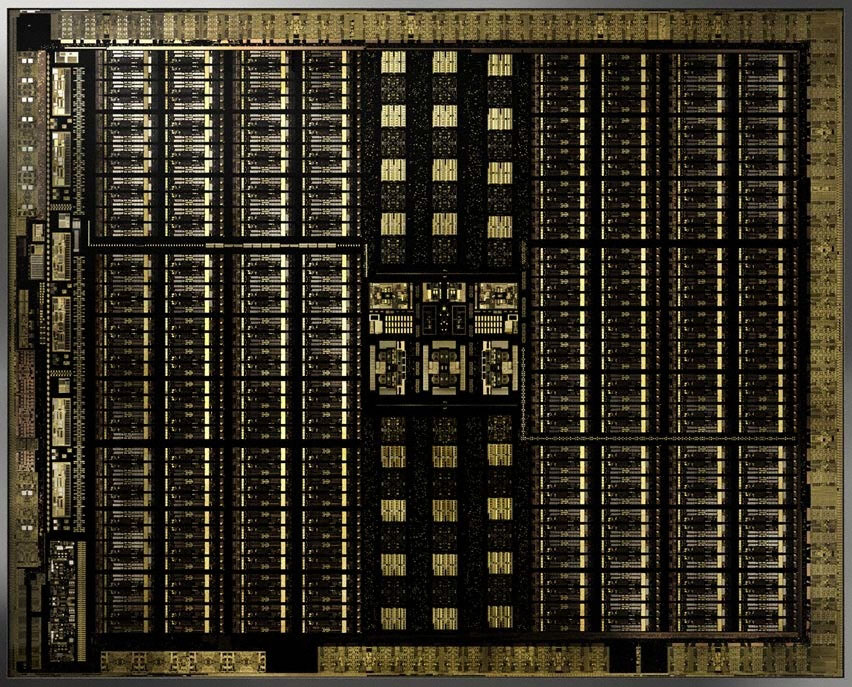
The centerpiece of today’s graphics-focused smorgasbord is TU102, a 754-square-millimeter GPU that sits at the heart of Nvidia’s GeForce RTX 2080 Ti. Its 18.6 billion transistors are fabricated on TSMC’s 12nm FinFET manufacturing process, which purportedly reflects a slight density improvement over TSMC’s previous 16nm node. The foundry even classifies 12nm technology under the same umbrella as 16nm on its website. We’re not accustomed to covering Nvidia’s “big” gaming GPU at the same time as a new architecture. But Nvidia knows that for real-time ray tracing to entice enthusiasts, it needs to run at smooth frame rates. Getting TU102 into the hands of early adopters was critical this time around.
Compared to the biggest Pascal-based GPU used in a desktop graphics card, GP102, Nvidia’s TU102 is 60% larger with a 55%-higher transistor count. But it’s not the company’s most massive processor. The Turing-based flagship is eclipsed by GV100, a 21.1 billion-transistor behemoth measuring 815mm². That GPU was introduced in 2017 with an emphasis on data center applications, and is still found on the $3000 Titan V.
TU102 is aimed at a different target market than GV100, and it’s consequently provisioned with a list of resources to match. While elements of Turing do borrow from Nvidia’s work in Volta/GV100, pieces of the architecture that either don’t benefit gamers or aren’t cost-effective on the desktop are deliberately stripped out.
Get Tom's Hardware's best news and in-depth reviews, straight to your inbox.
For example, each Volta Streaming Multiprocessor (SM) includes 32 FP64 cores for fast double-precision math, adding up to 2688 FP64 cores across GV100. They aren’t really useful in games though, and they eat up a lot of die space, so Nvidia pulled all but two of them from each Turing SM. As a result, TU102’s double-precision rate is 1/32 of its FP32 performance, leaving just enough FP64 compute to maintain compatibility with software dependent on it. Similarly, GV100’s eight 512-bit memory controllers attached to four stacks of HBM2 would have ended up being very expensive (just ask AMD about the trouble it had pricing HBM2-equipped Radeons competitively). They were consequently replaced with Micron-made GDDR6, facilitating a cheaper solution that’s still able to serve up a big bandwidth upgrade over Pascal-based predecessors.
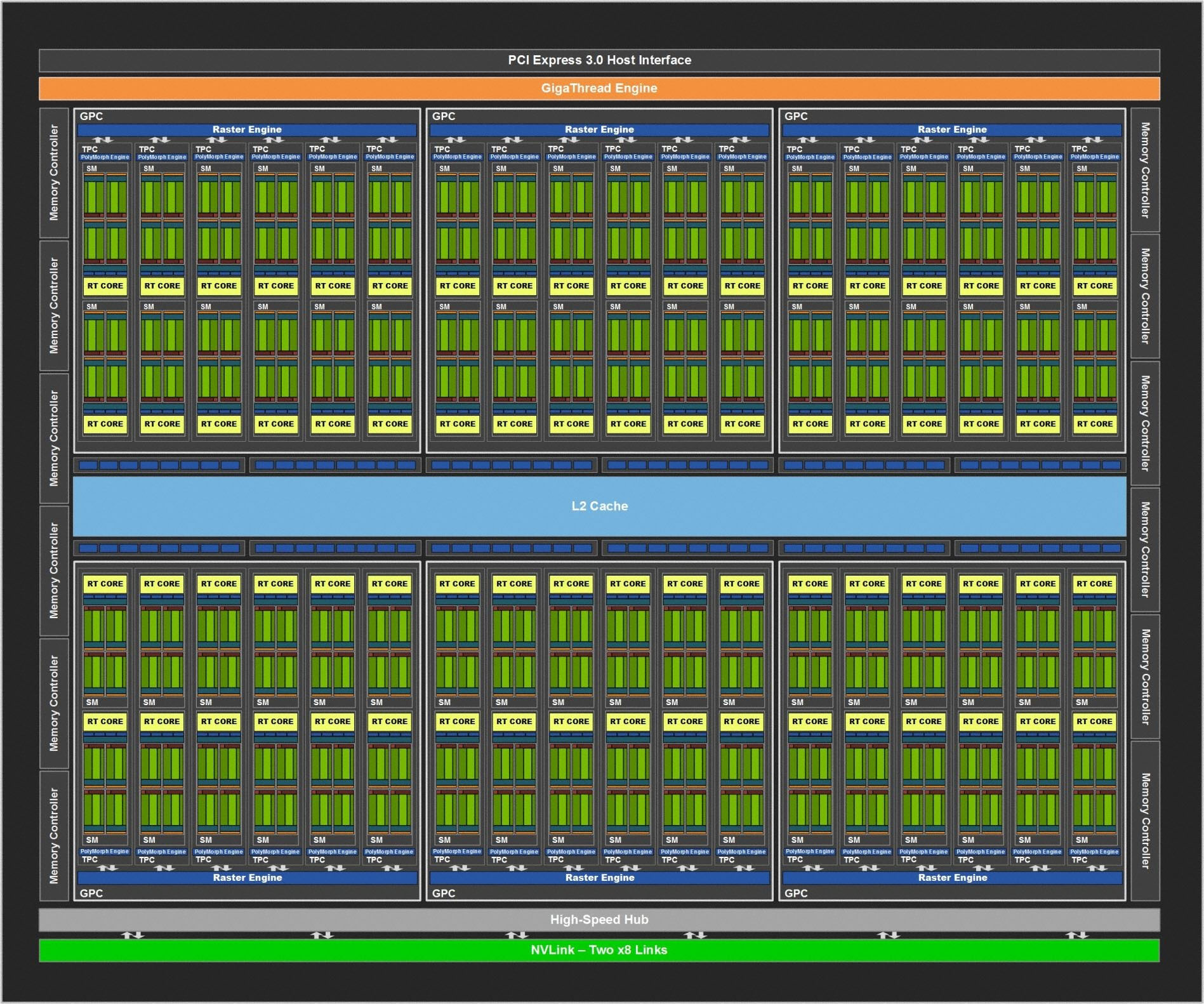
A complete TU102 processor comprises six Graphics Processing Clusters (GPCs) made up of a Raster Engine and six Texture Processing Clusters (TPCs). Each TPC is composed of one PolyMorph Engine (fixed-function geometry pipeline) and two Streaming Multiprocessors (SMs). Again, at the SM level, we find 64 CUDA cores, eight Tensor cores, one RT core, four texture units, 16 load/store units, 256KB of register file space, four L0 instruction caches, and a 96KB configurable L1 cache/shared memory structure.
Multiply all of that out and you get a GPU with 72 SMs, 4608 CUDA cores, 576 Tensor cores, 72 RT cores, 288 texture units, and 36 PolyMorph engines.
Those resources are fed by 12 32-bit GDDR6 memory controllers, each attached to an eight-ROP cluster and 512KB of L2 cache yielding an aggregate 384-bit memory bus, 96 ROPs, and a 6MB L2 cache.
Putting It All Together: GeForce RTX 2080 Ti
The TU102 found on GeForce RTX 2080 Ti isn’t a complete processor, though. Whether Nvidia wanted to leave room for a Titan-class model or found yields of fully-functional GPUs unsatisfactory above a certain bin, the RTX 2080 Ti has two of its TPCs disabled, leaving the card with 4352 CUDA cores, 544 Tensor cores, 68 RT cores, 544 texture units, and 34 PolyMorph engines.
Moreover, one of TU102’s 32-bit memory controllers is turned off, creating an aggregate 352-bit bus that moves data to 88 ROPs and 5.5MB of L2 cache. Nvidia matches its strategically-hobbled GPU to Micron’s MT61K256M32JE-14:A modules. Eleven of these populate the RTX 2080 Ti’s PCB, leaving one emplacement vacant. Nevertheless, theoretical peak bandwidth rises sharply compared to the previous generation cards due to GDDR6’s higher data rate: at 14 Gb/s on a 352-bit interface, you’re looking at 616 GB/s. In comparison, GDDR5X at 11 Gb/s held GeForce GTX 1080 Ti to 484 GB/s.
| Row 0 - Cell 0 | GeForce RTX 2080 Ti FE | GeForce GTX 1080 Ti FE |
| Architecture (GPU) | Turing (TU102) | Pascal (GP102) |
| CUDA Cores | 4352 | 3584 |
| Peak FP32 Compute | 14.2 TFLOPS | 11.3 TFLOPS |
| Tensor Cores | 544 | N/A |
| RT Cores | 68 | N/A |
| Texture Units | 272 | 224 |
| Base Clock Rate | 1350 MHz | 1480 MHz |
| GPU Boost Rate | 1635 MHz | 1582 MHz |
| Memory Capacity | 11GB GDDR6 | 11GB GDDR5X |
| Memory Bus | 352-bit | 352-bit |
| Memory Bandwidth | 616 GB/s | 484 GB/s |
| ROPs | 88 | 88 |
| L2 Cache | 5.5MB | 2.75MB |
| TDP | 260W | 250W |
| Transistor Count | 18.6 billion | 12 billion |
| Die Size | 754 mm² | 471 mm² |
| SLI Support | Yes (x8 NVLink, x2) | Yes (MIO) |
At least on the Founders Edition card, a base core frequency of 1350 MHz jumps all the way up to a typical GPU Boost rate of 1635 MHz, so long as GeForce RTX 2080 Ti is running cool enough. And because Nvidia cites peak compute performance using GPU Boost numbers, its top-end model achieves up to 14.2 TFLOPS of single-precision math.
The reference specification calls for a GPU Boost frequency of 1545 MHz and a slightly lower TDP. Whereas the Founders Edition card’s overclock imposes a maximum board power of 260W, reference-class implementations should duck in around 250W.
Both configurations feature two NVLink interfaces for multi-GPU connectivity, though. This technology is covered in greater depth further along, but in short, each x8 link enables 50 GB/s of bi-directional bandwidth to support higher resolutions and faster refresh rates. On GeForce RTX 2080 Ti, 100 GB/s of total throughput is enough for 8K monitors in Surround mode.
MORE: Best Graphics Cards
MORE: Desktop GPU Performance Hierarchy Table
MORE: All Graphics Content
Current page: Meet TU102 and GeForce RTX 2080 Ti
Next Page Meet TU104 and GeForce RTX 2080-
siege19 "And although veterans in the hardware field have their own opinions of what real-time ray tracing means to an immersive gaming experience, I’ve been around long enough to know that you cannot recommend hardware based only on promises of what’s to come."Reply
So wait, do I preorder or not? (kidding) -
jimmysmitty Well done article Chris. This is why I love you. Details and logical thinking based on the facts we have.Reply
Next up benchmarks. Can't wait to see if the improvements nVidia made come to fruition in performance worthy of the price. -
Lutfij Holding out with bated breath about performance metrics.Reply
Pricing seems to be off but the followup review should guide users as to it's worth! -
Krazie_Ivan i didn't expect the 2070 to be on TU106. as noted in the article, **106 has been a mid-range ($240-ish msrp) chip for a few generations... asking $500-600 for a mid-range GPU is insanity. esp since there's no way it'll have playable fps with RT "on" if the 2080ti struggles to maintain 60. DLSS is promisingly cool, but that's still not worth the MASSIVE cost increases.Reply -
jimmysmitty Reply21319910 said:i didn't expect the 2070 to be on TU106. as noted in the article, **106 has been a mid-range ($240-ish msrp) chip for a few generations... asking $500-600 for a mid-range GPU is insanity. esp since there's no way it'll have playable fps with RT "on" if the 2080ti struggles to maintain 60. DLSS is promisingly cool, but that's still not worth the MASSIVE cost increases.
It is possible that they are changing their lineup scheme. 106 might have become the low high end card and they might have something lower to replace it. This happens all the time. -
Lucky_SLS turing does seem to have the ability to pump up the fps if used right with all its features. I just hope that nvidia really made a card to power up its upcoming 4k 200hz hdr g sync monitors. wow, thats a mouthful!Reply -
anthonyinsd ooh man the jedi mind trick Nvidia played on hyperbolic gamers to get rid of thier overstock is gonna be EPIC!!! and just based on facts: 12nm gddr6 awesome new voltage regulation and to GAME only processes thats a win in my book. I mean if all you care is about is your rast score, then you should be on the hunt for a titan V, if it doesn't rast its trash lol. been 10 years since econ 101, but if you want to get rid of overstock you dont tell much about the new product till its out; then the people who thought they were smart getting the older product, now want o buy the new one too....Reply -
none12345 I see a lot of features that are seemingly designed to save compute resources and output lower image quality. With the promise that those savings will then be applied to increase image quality on the whole.Reply
I'm quite dubious about this. My worry is that some of the areas of computer graphics that need the most love, are going to get even worse. We can only hope that overall image quality goes up at the same frame rate. Rather then frame rate going up, and parts of the image getting worse.
I do not long to return to the day where different graphics cards output difference image quality at the same up front graphics settings. This was very annoying in the past. You had some cards that looked faster if you just looked at their fps numbers. But then you looked at the image quality and noticed that one was noticeably worse.
I worry that in the end we might end up in the age of blur. Where we have localized areas of shiny highly detailed objects/effects layered on top of an increasingly blurry background. -
CaptainTom I have to admit that since I have a high-refresh (non-Adaptive Sync) monitor, I am eyeing the 2080 Ti. DLSS would be nice if it was free in 1080p (and worked well), and I still don't need to worry about Gstink. But then again I have a sneaking suspicion that AMD is going to respond with 7nm Cards sooner than everyone expects, so we'll see.Reply
P.S. Guys the 650 Ti was a 106 card lol. Now a xx70 is a 106 card. Can't believe the tech press is actually ignoring the fact that Nvidia is relabeling their low-end offering as a xx70, and selling it for $600 (Halo product pricing). I swear Nvidia could get away with murder... -
mlee 2500 4nm is no longer considered a "Slight Density Improvement".Reply
Hasn't been for over a decade. It's only lumped in with 16 from a marketing standpoint becuase it's no longer the flagship lithography (7nm).


