Researchers Suggest That Semiconductors Can be Grown Instead of Printed
Researchers proposed a new method of manufacturing "the smallest structures in electronics".
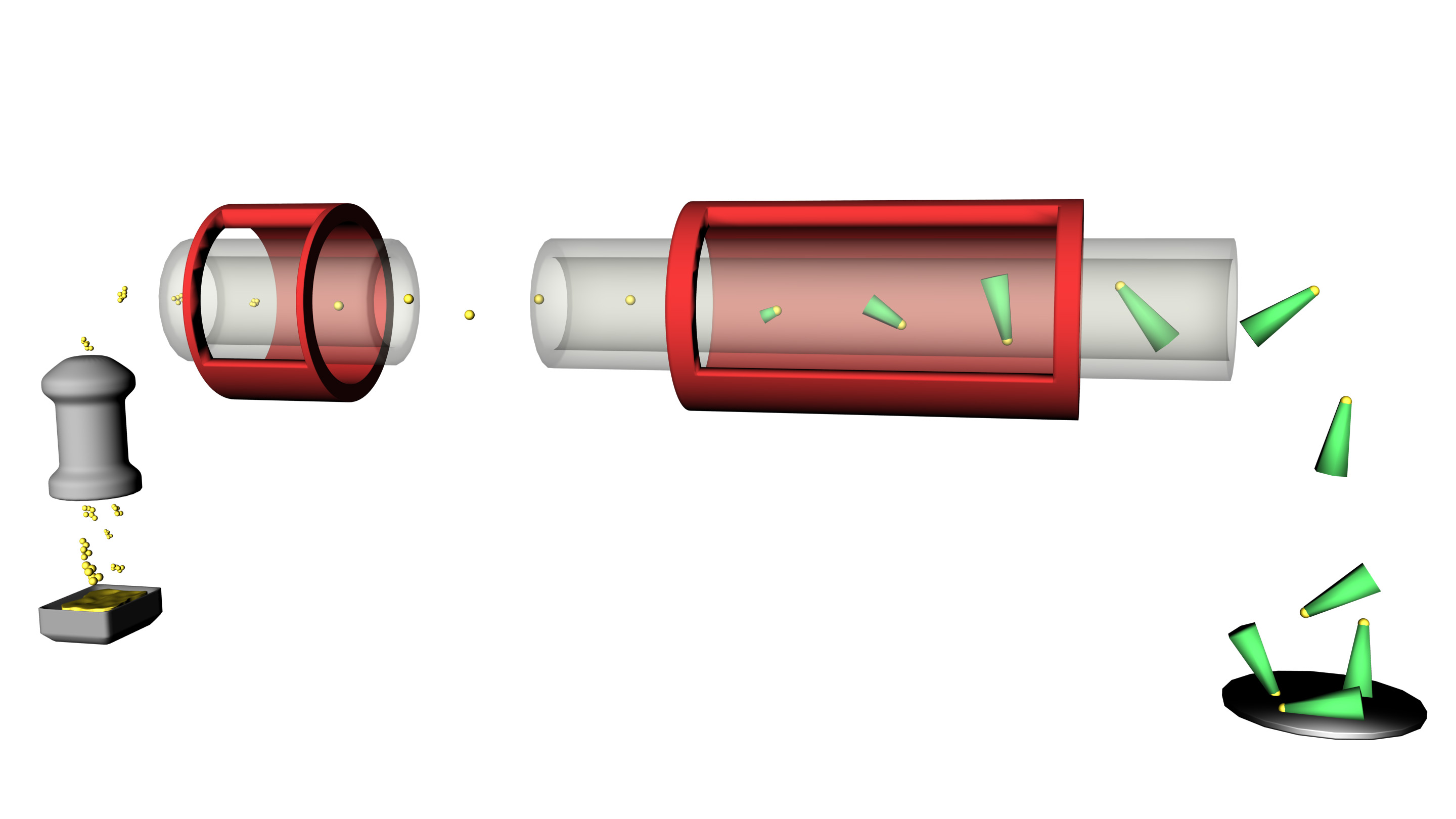
Rather than printing then on a silicon wafer, researchers propose to grow them while freely floating in a gas, and a self assembly method on surfaces. The project used gold nanoparticles inserted in a tube that acts as an oven to "bake" nanowires.
The method was developed at Lund University in Sweden and claims that the growth of the structures can be controlled using temperature, time and the size of the gold nanoparticles. "The basic idea was to let nanoparticles of gold serve as a substrate from which the semiconductors grow," said Lars Samuelson, who led the research. "This means that the accepted concepts really were turned upside down."
Samuelson said that his team has built a "prototype machine with a specially built oven", which demonstrates that the baking process "is not only extremely quick, [but] also continuous." At this, time the research project is following up to develop a method to capture the nanowires and "make them self-assemble in an ordered manner on a specific surface," such as glass or steel.
Article continues belowSamuelson believes that growing nanowires could be mature enough for semiconductor mass market production within two to four years.
Contact Us for News Tips, Corrections and Feedback
Get Tom's Hardware's best news and in-depth reviews, straight to your inbox.

Douglas Perry was a freelance writer for Tom's Hardware covering semiconductors, storage technology, quantum computing, and processor power delivery. He has authored several books and is currently an editor for The Oregonian/OregonLive.
-
SneakySnake I want to become a semiconductor farmer. I can nurture my little babies to full growth before they're ready for the big wide world of processing.Reply -
Onus Michael Crichton's "Prey" had an interesting take on this. Without spoiling (it's a good story), bacteria were used to poop out the desired semiconductors.Reply
-
groundrat This is a very interesting development. Eventually this may lead to 5nm architectures or smaller. It may make the manufacturing process less expensive as well... after the retooling.Reply -
southernshark GroundratThis is a very interesting development. Eventually this may lead to 5nm architectures or smaller. It may make the manufacturing process less expensive as well... after the retooling.Reply
They can already do 5nm................ and smaller as well at least in prototype.
What it should be able to do....... is allow much smaller companies to get into the game. Instead of needing a billion dollar facility to print wafers, a much smaller company could grow them. -
southernshark Of course one would still need a few million dollars to get set up, but compared with 1-2 billion....Reply
