SK Hynix Debuts 96-Layer '4D NAND' SSD With 64KB Bandwidth
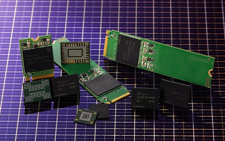
SK Hynix has announced its 96-layer "4D NAND" 512Gb (64GB) SSD chip, joining other vendors that have started manufacturing 96-layer 3D NAND products.
SK Hynix’s new 4D NAND SSD goes from the 72-layer technology the company used before to 96 layers. The company says this allows it to make 30 percent smaller chips with a 49 percent increase in bit productivity per wafer compared to its previous 72-layer 512Gb 3D NAND SSDs.
The product also has 30 percent higher write and 25 percent higher read performance than the older technology, and its data bandwidth has doubled to the industry’s biggest 64KB. Due to a new multiple gate insulators architecture, the drive’s data I/O speed reaches 1,200Mbps at 1.2V operation power.
SK Hynix uses charge trap flash (CTF), as opposed to floating gate, which is why the company calls its technology 4D NAND. The chip’s logic circuitry is placed underneath the flash cells. It calls this the Periphery Under Cell (PUC) technology. Other companies use similar technology, but call it something different. Micron calls it CMOS Under the Array (CUA), while Samsung calls it Core Over Periphery.
Future Roadmap
J.T. Kim, Vice President and Head of SK Hynix NAND Marketing, in a statement said: “This 96-Layer CTF-based 4D NAND ... will become a milestone in the company’s NAND Flash business, as a platform in developing future products. The company plans to start the early stage mass production of it within this year and further expand the production in M15 to actively respond to a variety of clients.”
SK Hynix plans to release other products that include the new 96-layer 4D NAND technology. These include a 1TB client SSD (this year) that will use the company’s own controllers and firmware, enterprise SSDs (second half of 2019) and UFS 3.0 storage products for the mobile market (first half of 2019).
The company said that it will also release “ultra-high density” 96-Layer 1TB triple-level cell (TLC) and quad-level cell (QLC) SSDs in 2019.
Get Tom's Hardware's best news and in-depth reviews, straight to your inbox.
Lucian Armasu is a Contributing Writer for Tom's Hardware US. He covers software news and the issues surrounding privacy and security.
-
bit_user Reply
What? What is the point about 64 KB bandwidth? Most of the article makes sense, but I'm still not clear on this point.21461208 said:Sky Hynix Debuts 96-Layer '4D NAND' SSD With 64KB Bandwidth -
Olle P Should it read bus-width?Reply
Seems a bit much, but would also explain the high data transfer speed.
The "bandwidth of 64KB" comes straight from the press release. -
bit_user Reply
Yeah, I wondered if they were talking about something like that. Thanks for pointing it out.21462833 said:Should it read bus-width?
Seems a bit much, but would also explain the high data transfer speed.
The "bandwidth of 64KB" comes straight from the press release.
I'm rather surprised to see something like this from Lucian. A good journalist should be a filter for this kind of thing and hopefully reach out to their PR department for clarification. The quality of his articles is normally very good.
