TSMC Places Massive EUV Tools Order to Boost Capacity
When it comes to EUV installations, TSMC is ahead of the industry.

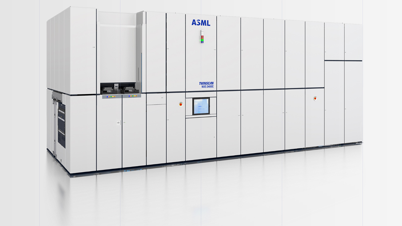
Earlier this year, TSMC (Taiwan Semiconductor Manufacturing Co.) said that it had deployed around 50% of all extreme ultraviolet (EUV) lithography tools installed and run worldwide, which means that it uses more EUV machines than any other company in the industry. According to a Digitimes report, TSMC plans to stay ahead and has already placed an order for over a dozen of ASML's Twinscan NXE EUV scanners due to be delivered next year.
13 EUV Tools Ordered, More Needed
TSMC has placed orders for 'at least' 13 EUV systems with ASML, reports DigiTimes citing undisclosed industrial sources. These tools are set to be delivered throughout 2021, though exact delivery and installation schedule is unknown. Meanwhile, TSMC's actual needs for next year might be as high as 16 – 17 EUV scanners as the company is ramping up production using its fabrication technologies that feature EUV layers. TSMC has not confirmed the report.
At present, TSMC uses ASML's Twinscan NXE EUV scanners to make commercial chips at its N7+ as well as N5 nodes, but in the next few quarters the company will add N6 (which is actually set to enter HVM in Q4 2020 or Q1 2021) as well as N5P processes that also feature EUV layers.
TSMC's needs for EUV tools are increasing as its technologies get more complex and employ more layers that need to be processed using extreme ultraviolet lithography tools. TSMC's N7+ uses EUV for up to four layers in a bid to reduce usage of multi-patterning techniques when making highly complex circuits.
The N6 technology will expand usage of EUVL to five layers (while retaining IP compatibility with DUV-only N7), whereas TSMC's flagship N5 node can use EUVL for up to 14 layers. The upcoming N4 is expected to increase the maximum number of EUV layers further, whereas in case of N3 (due to be available in 2023) that number will grow to over 20.
According to ASML, one EUV layer required one Twinscan NXE scanner for every ~45,000 wafer starts per month in 2018 ~ 2019. As productivity of tools increases, the number of WSPMs grows. Therefore, to equip a GigaFab (with a production capacity higher than 100,000 wafer starts per month) that is set to make chips using N3 or more advanced nodes, TSMC needs at least 40 EUV tools in that fab.
Earlier this week TSMC's board of directors approved spending of $15.1 billion on new production tools, fab construction, installation of specialty technology capacity, upgrading its advanced packaging facilities, and R&D in Q1 2021. Some of the approved funds might be used to purchase EUV tools.
Get Tom's Hardware's best news and in-depth reviews, straight to your inbox.
ASML Boosts EUV Production Capacities
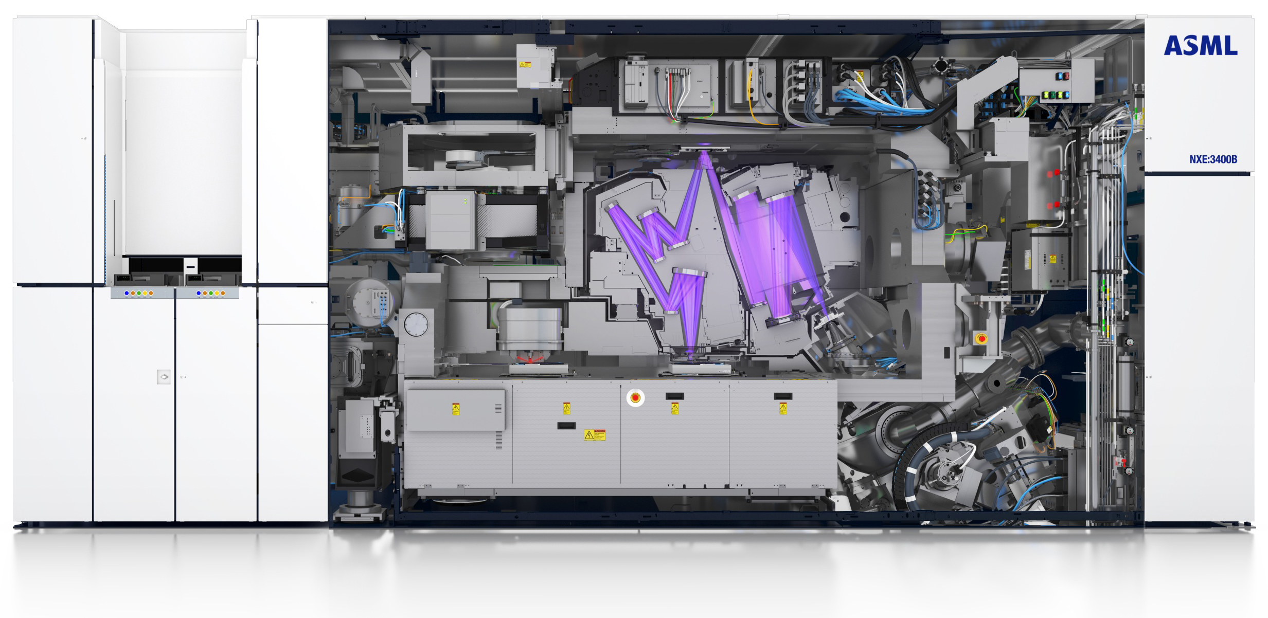
ASML's latest Twinscan NXE:3400B and NXE:3400C step-and-scan system are quite expensive. Back in October ASML revealed that four EUV systems in its order book were worth €595 million (~$703 million), so a single piece of equipment can cost as much as €148.75 million ($175.75 million). That said, 13 EUV sets may cost TSMC a whopping $2.284 billion.
But money is not the only concern when it comes to EUV tools. ASML is the single company that produces and installs EUV scanners and it has a relatively limited production and installation capacity. After all the adjustments of its manufacturing process, the company believes it can shrink cycle time for a single machine to 20 weeks, which would result in per annum capacity of 45 to 50 systems.
Throughout three quarters this year, ASML has shipped 23 EUV scanners and intends to sell a little less than the 35 systems it originally planned for 2020. So far, ASML has shipped 83 commercial EUV tools (which includes NXE:3350B, NXE:3400B, and NXE:3400C machines sold from Q1 2015 to Q3 2020) to all of its customers.
Ahead of the Industry
If TSMC's claims about ownership of ~50% of all Twinscan NXE tools installed and ran worldwide are correct, the company may already own from 30 to 40 EUV scanners, which is more than any other company in the industry.
TSMC is certainly not the only maker of semiconductors that procures a large number of EUV tools. Samsung is believed to be somewhat behind as the company only uses EUV to make its 7LPP and 5LPE SoCs as well as some DRAMs. But as Samsung Foundry expands usage of EUVL for logic, whereas Samsung Semiconductor boosts production of EUV-based DRAM, the conglomerate will inevitably have to start purchasing more Twinscan NXE scanners.
Intel is also expected to start deploying EUVL systems sometimes in 2022 when it starts making chips using its 7 nm node. While there are many uncertainties about this process technology as well as Intel's plans going forward, it is inevitable that the company will also be one of the major EUVL adopters in the coming years.
Other major customer for ASML's Twinscan NXE machines will be SK hynix, which already test drives these tools and develops appropriate nodes and DRAM ICs.
China's biggest contract maker of chips, SMIC, still cannot get its already purchased EUV tool because of the Netherlands's export requirements. Meanwhile, since it is close to impossible for the company to procure other fab tools necessary for EUV production from companies based in the U.S., it does not really need more than one EUV scanner just now.
Micron plans to avoid usage of EUVL for several upcoming DRAM generations, but since it will still have to transit to EUV-enabled nodes eventually, it will likely procure at least one Twinscan NXE system in the coming years for development purposes.
It is inevitable that demand for EUV tools is only going to increase in the coming years, but from where we stand today, TSMC is going to remain the main adopter of these scanners for the foreseeable future with Samsung and Intel following.

Anton Shilov is a contributing writer at Tom’s Hardware. Over the past couple of decades, he has covered everything from CPUs and GPUs to supercomputers and from modern process technologies and latest fab tools to high-tech industry trends.
-
neojack i always wonder why ASML does not inflate the price of their tools over the top.Reply
they are unique, they could sell them 1B each or something. sky is the limit. they have a monoply on a technology everyone wants.
or maybe their management is more interested into the greater good and not just capitalism ?
not complaining for sure. don't want having to pay 5000$ for a CPU. -
InvalidError Reply
ASML cannot sell equipment to its customers at stupid markups because most of its clients are also R&D partners, investors and in many cases, they are also on the board of directors. In other words, foundries are basically outsourcing their equipment R&D to ASML instead of individually reinventing the photolithography wheel in exchange for fair pricing. Intel divested itself of some of its ASML holdings in 2018 and still has a ~3% stake in it.neojack said:i always wonder why ASML does not inflate the price of their tools over the top.
they are unique, they could sell them 1B each or something. sky is the limit. they have a monoply on a technology everyone wants.
Intel also divested part of its ASML stake back in 2012, which coincides with the beginning of Intel's process slip-ups. -
neojack i didn't know that, very interesting ! take a likeReply
maybe we can deduce that intel's moving away from TSMC also costed them R&D efforts. they turned their backs from ASML because of their hubris
2014 intel : "we are the best fab in the world and we do not need subcontractors like ASML". "our 14nm is the best !"
2020 intel : still on 14nm, struggling with their 10nm. -
GoalTorrent Reply
What is the status of the photoresist being used at TSMC or any other company using EUVL? There are several in the running, but almost nothing published on who seems to have gained the place in the fab.Admin said:TSMC reportedly buys over a dozen of ASML Twinscan NXE EUV machines
TSMC Places Massive EUV Tools Order to Boost Capacity : Read more -
jkflipflop98 Replyneojack said:i didn't know that, very interesting ! take a like
maybe we can deduce that intel's moving away from TSMC also costed them R&D efforts. they turned their backs from ASML because of their hubris
2014 intel : "we are the best fab in the world and we do not need subcontractors like ASML". "our 14nm is the best !"
2020 intel : still on 14nm, struggling with their 10nm.
Uh, what? That makes no sense. Intel uses plenty of everyone's tools. Including ASML. -
InvalidError Reply
While Intel may use ASML stuff, the reason Intel is in its current predicament is because it thought it could leapfrog ASML by aggressively refining the equipment it already had and it has turned into a mostly unmitigated failure so far. Had Intel retained the same level of partnership it had with ASML before 2012, maybe it wouldn't have fallen as far behind.jkflipflop98 said:Uh, what? That makes no sense. Intel uses plenty of everyone's tools. Including ASML. -
jkflipflop98 ReplyInvalidError said:While Intel may use ASML stuff, the reason Intel is in its current predicament is because it thought it could leapfrog ASML by aggressively refining the equipment it already had and it has turned into a mostly unmitigated failure so far. Had Intel retained the same level of partnership it had with ASML before 2012, maybe it wouldn't have fallen as far behind.
Again, that makes no sense. Guess who had these EUV tools before TSMC? Intel. Lithography is always being researched and worked on. It's the hard part of making chips. It's not like all that research is going to waste. You can apply the same tricks you learned at 190nm to the newer wave. -
InvalidError Reply
AFAIK, Intel only plans to start using EUV for 7nm in 2021, everything it currently has in production is still DUV with increasingly fancy multi-patterned computational lithography.jkflipflop98 said:Again, that makes no sense. Guess who had these EUV tools before TSMC? Intel. -
InvalidError Reply
If you do a simple search for Intel and EUV, the only results you get are related to 7nm. Even Tiger Lake on 10nm+ is still quad-patterned DUV. The only EUV "production" Intel currently has is R&D to (hopefully) figure 7nm out before the remainder of its EUV equipment rolls in and the six months slip on 7nm launches suggests it may not be going well.jkflipflop98 said:You heard wrong, dude.


