AMD's Zen 2 FPU for PlayStation 5 is 35% smaller than a Ryzen 7 3800X but sacrifices nothing in terms of gaming performance
Just chop off what you don't need.

Chips and Cheese acquired a Zen 2 CPU used in Sony's PlayStation 5 and went to town studying differences compared to AMD's Ryzen-branded products sporting the same CPU architecture (like the Ryzen 3000 series). The chip review outlet found that Sony's custom-designed Zen 2 chip sports a heavily cut-down FPU that's shrunk by 35%. However, Chips and Cheese discovered these changes don't impact gaming performance making it the "perfect" gaming CPU.
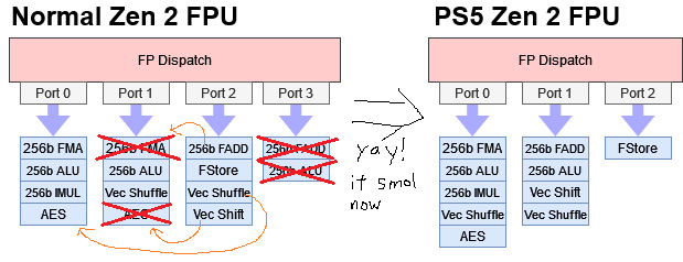
The area AMD paid the most attention to when designing Sony's custom Zen 2 PlayStation 5 CPU was the FPU, or floating point unit. AMD cut down the number of floating point pipes and eliminated some of the FP/vector execution units. Compared to a comparable Zen 2 Ryzen CPU desktop chip like the Ryzen 7 3700X or 3800X, Sony's custom Zen 2 chip comes with only half of the FPU capabilities of a 3700X or 3800X.
To do this, AMD added more functionality to the remaining floating-point ports. In a traditional Zen 2 chip, there are four ports, with most of the ports handling duplicate instructions. But with the PS5 CPU, all of the duplicates have been deleted with the fourth port being deleted entirely. Port 0 and 1 handle all of the instructions while port 2 only handles FStore.
AMD also shrank the register file to improve size efficiency. The amount of blocks the register file has is the same as AMD's Ryzen 3000 chips, but each block size is smaller. Chips and Cheese believes this was a design change made in conjunction with the FPU port count reduction apparently because the performance impact of a smaller register file size is directly correlated with the FPU's capabilities.
Chips and Cheese found that these changes did not make any difference in terms of gaming performance. In a test with Call of Duty: Black Ops - Cold War Zombies, the chip review outlet monitored the FPU execution units and found that none of the EUs were taxed beyond 20-22%. The only benchmarks where the FPU nerfs compromised performance were in heavy productivity/synthetic tests such as Y-Cruncher. But even in Y-Cruncher performance only dropped by 16% (compared to a normal Zen 2 chip) despite having effectively half of the FPU execution pipeline of a traditional Zen 2 CPU.
With these changes, AMD was able to reduce Sony's PS5 Zen 2 FPU size by a whopping 35% while offering identical gaming performance as Zen 2 chips (at identical clock speeds and memory speeds that is). It's an excellent representation of AMD being able to custom-design chips specifically for its customers. Though interestingly these specific changes have only been done to Sony's PS5 CPU, and no other custom chips AMD makes currently (including the Steam Deck's Van Gough APU).
This design appears to be working great for Sony. Leaked specifications of the PlayStation 5 Pro suggest that Sony will keep using this same Zen 2 chip, but with a dual-mode performance mode that allows developers to clock the CPU to 3.85 GHz if necessary.
Get Tom's Hardware's best news and in-depth reviews, straight to your inbox.

Aaron Klotz is a contributing writer for Tom’s Hardware, covering news related to computer hardware such as CPUs, and graphics cards.
-
gg83 What about the Xbox chip? Did Microsoft keep the fpu the same? Or is it so similar there's no sense in mentioning?Reply -
usertests Great article and everyone should be reading Chips and Cheese (or at least glance at it every week or two to see what's being covered).Reply
The article notes that AMD has not had to do the same thing for Zen 4c, you get everything in the full core but clock speed, and then less L3 cache. I wonder if a future PS6/Xbox would take both approaches at the same time. -
thestryker Reply
The CPU portion of the Xbox Series X/S die is the same as Zen 2 so they didn't have AMD make any changes.gg83 said:What about the Xbox chip? Did Microsoft keep the fpu the same? Or is it so similar there's no sense in mentioning? -
igor_kavinski https://forums.anandtech.com/threads/zen-5-discussion-epyc-turin-and-strix-point-granite-ridge-ryzen-8000.2607350/post-41178489Reply
The FPU is 35% smaller, not the CPU! -
Reply
The chip review outlet found that Sony's custom-designed Zen 2 chip sports a heavily cut-down FPU enabling the CPU to be shrunk by 35%.
AMD's Zen 2 CPU for PlayStation 5 is 35% smaller than a Ryzen 7 3800X
Seriously ? Where does the original article state this ? It's the FPU's size they are talking about, NOT the CPU.
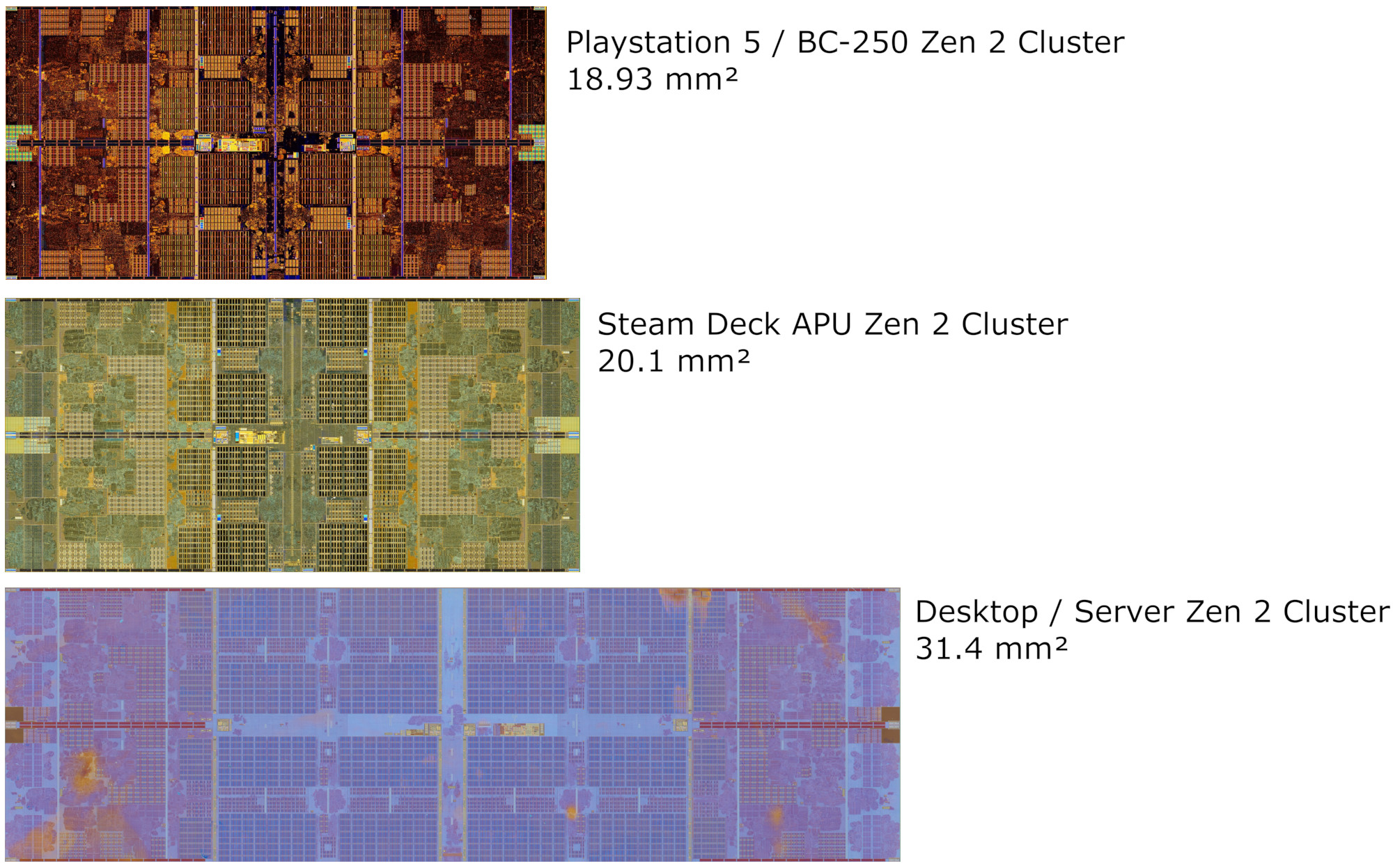
Though, size of a quad core cluster only goes down by 5.8%. That’s not enough to enable a dramatic core count increase or a much smaller and cheaper die. -
bit_user I've got to say it: I feel somewhat vindicated. I predicted there's no way PS5 would have 8x full Zen 2 cores, and I was (technically) right!Reply
Thanks to Brutus, I got to take a closer look at just how AMD got Zen 2’s FPU to drop from 0.91 to 0.59 mm2.
Sony/AMD: Et tu, Brute?
(Sorry, I had to say that too!)
: D -
bit_user Reply
Yes, if you're into that sort of thing. It replaced Anandtech as my go-to for deep architecture-level analysis & microbenchmarking, but they do it even better!usertests said:everyone should be reading Chips and Cheese (or at least glance at it every week or two to see what's being covered).
And if you're a regular reader, please chip in a couple $/mo to support C&C on Patreon. They're ad-free, so entirely donation-supported. -
bit_user Reply
I imagine Aaron Klotz skimmed the C&C article too quickly and got to the part with the die size comparison:Metal Messiah. said:Seriously ? Where does the original article state this ? It's the FPU's size they are talking about, NOT the CPU.
Though, size of a quad core cluster only goes down by 5.8%. That’s not enough to enable a dramatic core count increase or a much smaller and cheaper die.
I don't see where C&C comes out and says it, but the vast majority of the cluster size reduction seems due to the reduction in L3 cache between the APU-oriented clusters vs. desktop/server clusters. As you state, they do explicitly specify that the cores, themselves, only shrunk by 5.8%. Furthermore, we know Zen 2 APUs have half the L3 cache per core as their desktop cousins. -
usertests Reply
Alternatively he picked up the Zen 4c tidbit. There were two 35% reductions in the article to get confused by!bit_user said:I imagine Aaron Klotz skimmed the C&C article too quickly and got to the part with the die size comparison:
A 35% reduction in FPU area by itself is impressive. But the size of a quad core cluster only goes down by 5.8%.
A smaller clock mesh and other optimizations let Zen 4c achieve a 35% area reduction for the entire core, not just the FPU.
35% is the core size reduction for Zen 4c from Zen 4, not taking into account different amounts of L3 cache. -
gg83 Reply
So the clusters aren't the entire chip?bit_user said:I imagine Aaron Klotz skimmed the C&C article too quickly and got to the part with the die size comparison:
I don't see where C&C comes out and says it, but the vast majority of the cluster size reduction seems due to the reduction in L3 cache between the APU-oriented clusters vs. desktop/server clusters. As you state, they do explicitly specify that the cores, themselves, only shrunk by 5.8%. Furthermore, we know Zen 2 APUs have half the L3 cache per core as their desktop cousins.

