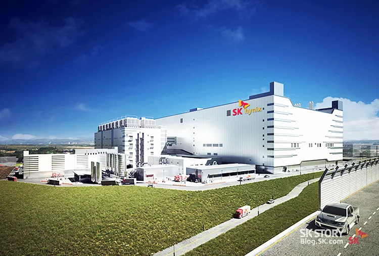
SK hynix is planning to build a $4 billion chip packaging facility in West Lafayette, Indiana, reports the Wall Street Journal. The fab is set to start operations in 2028 and create up to 1,000 jobs. This move, potentially backed by state and federal tax breaks, is part of SK hynix's efforts to strengthen its positions as a manufacturer of non-commodity memory.
The investment in the Indiana facility represents a strategic step for SK hynix to improve its advanced chip packaging capabilities. Such advanced memory packaging technologies could be used to build high-bandwidth memory, which is an important ingredient in many artificial intelligence and high-performance computing applications.
"[SK hynix] is reviewing its advanced chip packaging investment in the U.S., but hasn’t made a final decision yet," a company spokeswoman told the WSJ.
If the project gets the greenlight from SK hynix, the advanced pacakaging facility will start operations in 2028 and will create up to 1,000 jobs. Given the planned cost of the fab — $4 billion — the plant will be one of the world's largest advanced packaging facilities. Government support is crucial for this investment, with possible state and federal tax incentives, the report says. These incentives are part of a larger effort to strengthen the U.S. semiconductor industry and reduce reliance on foreign suppliers.
SK hynix is one of the suppliers of HBM memory to Nvidia, which builds AI GPUs that are vital for powering advanced AI services like ChatGPT. The recently revealed Nvidia Blackwell B200 will use eight HBM3e chips per GPU. This collaboration highlights SK hynix's role in the supply chain of critical components for the AI industry.
The broader context of this investment highlights the U.S. government's efforts to advance domestic chipmaking capabilities using initiatives like the CHIPS and Science Act. This act, which recently provided $8.5 billion in direct government funding to Intel, is instrumental for enhancing the U.S. semiconductor industry's competitiveness, especially amid rising competition and trade wars with China. SK hynix's planned facility in Indiana is a significant development in this context, contributing to the growth and resilience of the U.S. semiconductor sector.
Government funding for various domestic chip manufacturing and packaging endeavors has been a bit sluggish, so the current situation represents more of a statement of intent rather than a finalized deal. Whether it will move on to the construction phase remains to be seen.
