APC BN650M1-CA UPS Tear-Down
More Cable Management
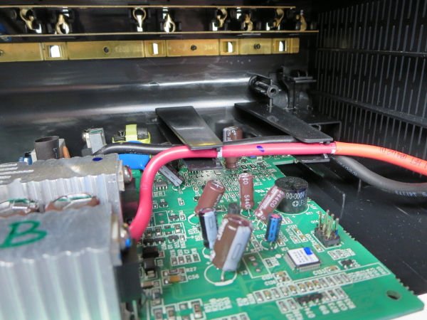
To protect the PCB’s battery wire solder joints, the battery wires clip into two tall supports along the way.
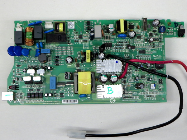
The green ‘B’ on top of the heat sink and streak across the top of capacitors located between heat sinks suggests that there was a second QA stage. Most heat sink screws have both blue and green marks as well, hinting that APC may have had issues with too many field failures caused by missing screws.
Ground Strip
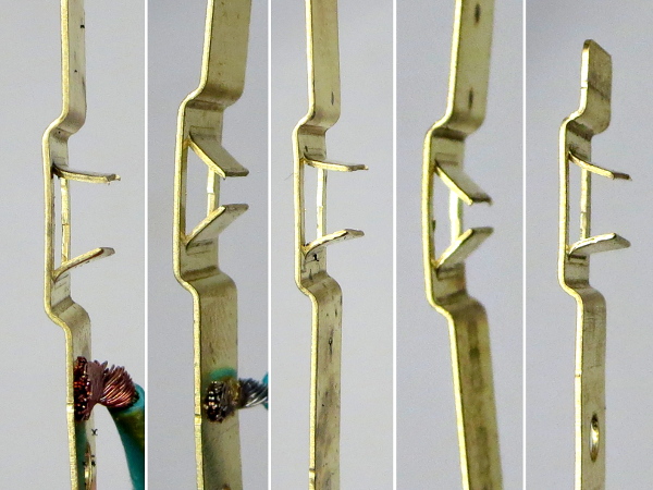
The ground strip is of the disappointing bent-flap type. Why is that a let-down? Because those flaps tend to suffer from plastic (permanent) deformation when ground pins are inserted, and they may develop intermittent contact after only a few insert-remove cycles. If some of those contacts look like they may have been abused to you, then you'll be horrified to learn that this is actually their factory-new state. I haven’t attempted to use the UPS in any way yet. The only explanation I can think of is that locations looking like they were plowed through must have been used for factory testing.
Article continues belowAs you can see, the ground wires are spot-welded to the strip. The battery backup live and neutral strips also have their wires spot-welded.
Traditional Soldering
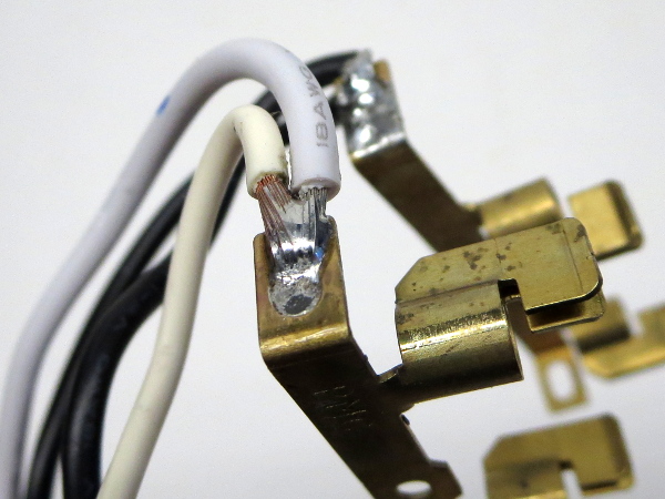
As usual, we get pinchy fingers for the live and neutral strips. There's no fancy high-current contact welding for the always-on surge-only outlets, just two plain old wire pairs. One is bare copper coming directly from the power cord or breaker, and the other is tin-plated copper going to the board connector, joined together by solder blobs on brass strips. Whatever surge protection these two get comes from the cord’s in-line common-mode choke and whatever is on the board’s input protection.
Shrouded
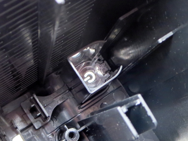
To limit the amount of light bleed from the status LED through the UPS’ side vents and other openings, the power button and its LED are surrounded most of the way around by a plastic shroud. I would call this a little more elaborate than the BGE90M’s piece of heat-shrink tubing and acrylic light guide stem.
Inside-Out
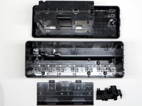
Flipped inside-out, the battery bay clearly dominates the BN650's internal volume. Between the battery bay and cord entry point to the right, there is a fair amount of wasted space that could have been filled by a longer battery or eliminated by omitting the two always-on surge-only outlets, shortening the chassis, and re-distributing leftover space between the remaining outlets.
Get Tom's Hardware's best news and in-depth reviews, straight to your inbox.
If you are curious about the date indicated by the dials, it is April 2016, just one month prior to launch.
Board – Top
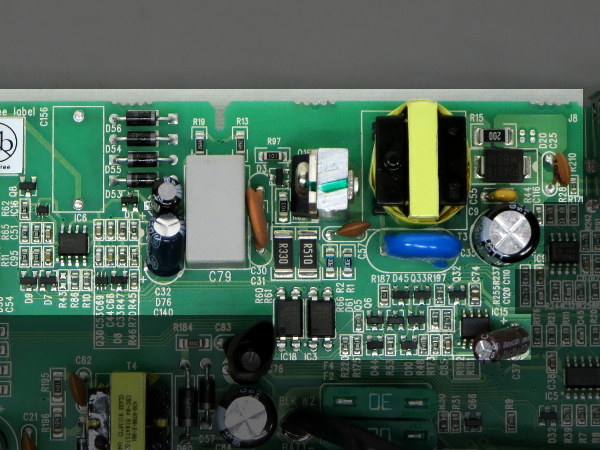
There is one thing that stands out in this design: there are two discrete diode bridges, each next to a small transformer, output diodes, and an output filter capacitor. The BN650M1 has dual input power supplies for some reason. Can you guess why that might be?
Board Bottom
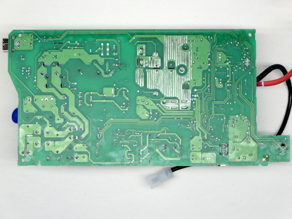
Were you expecting to see more components hidden under the board? You shouldn’t, since none of the APC UPSes I have taken apart had any. As usual for APC, the soldering work is as good as it gets (though there's a slight amount of flux residue along the top edge).
Do you see the two fat traces going up from the three large pads near the bottom-right corner? One-third of the way up, they jump to the other side and connect to the two other fat traces going to the left. These connect the two power supplies’ output capacitors together. Both supplies power a single rail.
Input Protection
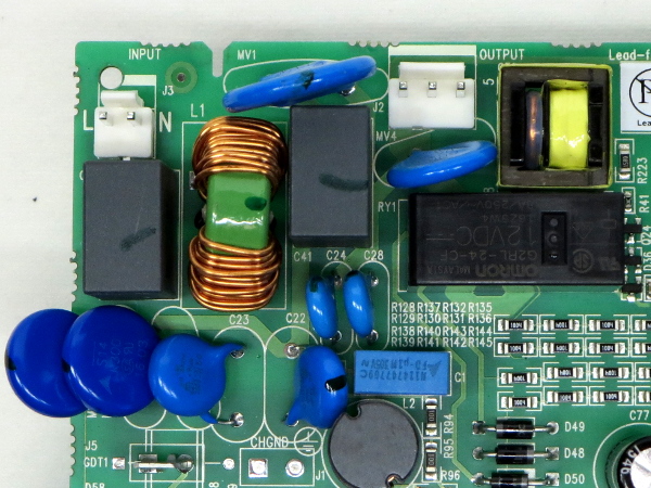
There are a few more MOVs and capacitors along the AC power path than average, starting with 1 µF Illinois X2 caps flanking the common-mode choke on both sides. It's followed by a 20D360K and a pair of S14K300 MOVs paired with four X1Y1-class caps before reaching the Omron DPDT relay, which switches the output between direct AC and inverter output. Finally, before passing through the current-sensing transformer, a 14D241K MOV provides one last layer of surge protection near the battery backup outlet cable’s connector.
That’s the most elaborate EMI filtering and surge suppression I have seen in a consumer-grade UPS since my old BX1000.
Small Power Supply
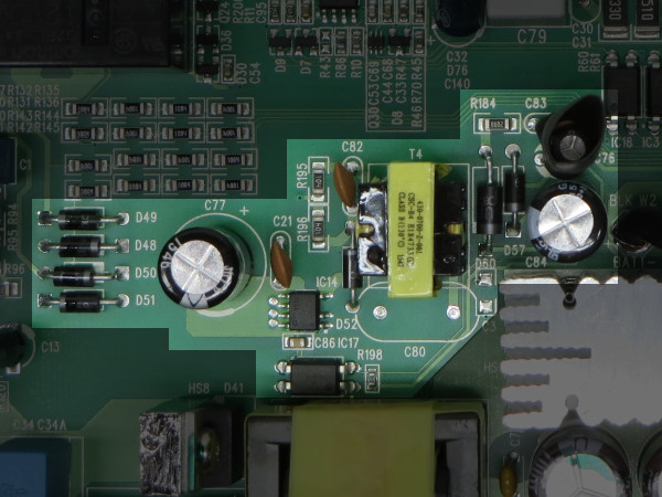
What we have here is a high-efficiency standby supply based on Power Integration’s LNK364 in a design that closely follows the datasheet's example application. This chip is intended to provide 6 W of output power from an 85-265 VAC universal input supply range, withstand input voltages up to 700 V, and consume less than 300 mW under no-load condition to meet energy efficiency standards. Unlike the reference design, APC’s implementation is missing the EMI suppression Y-cap.
Following the power traces feeding its input rectifier bridge reveals that the supply draws power directly from the AC input connector. That makes sense if you want to recover from a dead battery or trickle-charge it even while the unit is off. I expect to see sub-watt off-state power consumption.
Running Power Supply
The main power supply uses a more conventional design based on a 3843 switching controller (possibly from TI, based on the pin locator strip) driving an external STP5NK60Z switching FET rated for 650 V/5 A/1.6 Ω. Its input rectifier is built from regular axial 1N4007 diodes and uses a 0.1 µF polypropylene metal film capacitor combined with two ceramic caps for filtering, which is surprisingly little. One 47 µF Jianghai and one 4.7 µF Chang capacitor, both rated for 50 V, provide filtering for the 3843’s bootstrap power supply, while a 330 µF, 35 V Chang capacitor (same as the small supply) provide filtering at the output.
Tracing the diode bridge’s input reveals that it is powered from the output connector, which means it gets no power while the relay is in the normally closed position (off/inverter) and the inverter is not running. How much power does this arrangement waste while on battery?
MORE: CyberPower EC350G Tear-Down
MORE: APC BGE90M-CA Tear-Down
MORE: APC BE550G Tear-Down
-
firefyte I'm not sure if you found this spec sheet for the battery:Reply
http://www.csb-battery.com/upfiles/dow01320199159.pdf
I must comment, however, that I thoroughly enjoy these teardowns, as I had no idea that they can be THAT bad (or good). -
Daniel Sauvageau Reply
Yes, I did find that battery. Despite the model number differing by only one character, the HC-1228 is a much bigger battery (2.5kg vs 2.06kg, that's over 20% heavier) and if you look at the top, the terminal locations are completely different as well. Not comparable at all.18577258 said:I'm not sure if you found this spec sheet for the battery:
http://www.csb-battery.com/upfiles/dow01320199159.pdf
I must comment, however, that I thoroughly enjoy these teardowns, as I had no idea that they can be THAT bad (or good).
Glad you liked it.
-
nukemaster Glad you did this since you mentioned this unit in the comments on the other tear-down.Reply
Looks like the 75 watt unit(when on sale) is the better buy(as long as you do not need the ground and are power low light loads anyway). -
Daniel Sauvageau Reply
Yes, for small loads, the BGE90M is a pretty nice catch and I'm glad I picked two of them up at a ridiculously low price. I'll be swapping out my mother's BE550 with one of them the next time I drive there.18577935 said:Looks like the 75 watt unit(when on sale) is the better buy(as long as you do not need the ground and are power low light loads anyway).
When you buy a $100+ black box, aren't you at least the least bit curious about what's inside, what you are actually getting for your money? If you aren't, nobody is forcing you to read my tear-downs. Feel free to skip.18579009 said:What's the point of these teardowns? -
nukemaster Reply
Some people just like to take things apart and look inside. For others these types of articles are much safer.18579009 said:What's the point of these teardowns?
I am always interested in seeing inside of this type of stuff(any electronics for that matter.). -
nukemaster Reply
It is just just APC.18580671 said:But it seems like they only teardown apc's. Why only them?
Here are some Cyber Power units
http://www.tomshardware.com/picturestory/700-cyberpower-lx1500gu-fc-ups-tear-down.html
http://www.tomshardware.com/picturestory/731-cyberpower-ec350g-ups-tear-down.html#xtor=RSS-100
http://www.tomshardware.com/picturestory/721-cyberpower-cp1000pfclcd-ups-tear-down.html
I think it is limited to what the reviewer can buy(maybe locally as well) as well. -
Daniel Sauvageau Reply
Best Buy Canada stocks mostly CyberPower. Staples Canada stocks mainly APC. There are the odd Tripp-Lite units here and there, but after the SMART1000, I'm not going to try my luck with Tripp-Lite again unless I find heavily discounted units or receive a review sample.18580671 said:But it seems like they only teardown apc's. Why only them?
www.tomshardware.com/picturestory/708-tripp-lite-smart1000lcd-tear-down.html
On Amazon.ca, the SMART1000LCD is currently listed at $215 and there are some clearly superior UPS available around $160. I try to avoid buying UPS from Amazon due to their no-return/exchange/refund policy on UPS.
