ABS Ultimate X9 Firefox Extreme - Gaming Performance for Less
Deals
By
Darren E. Polkowski
published
Add us as a preferred source on Google
Stay On the Cutting Edge: Get the Tom's Hardware Newsletter
Get Tom's Hardware's best news and in-depth reviews, straight to your inbox.
By submitting your information you agree to the Terms & Conditions and Privacy Policy and are aged 16 or over.
You are now subscribed
Your newsletter sign-up was successful
An account already exists for this email address, please log in.
Subscribe to our newsletter
Memory Timings
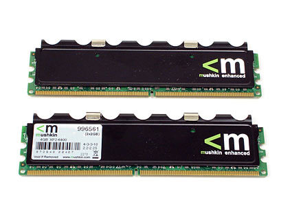
Inside were two Mushkin XP2-6400 2 GB modules
Swipe to scroll horizontally
| Header Cell - Column 0 | Memory Timing | ABS | iBuyPower | Falcon-NW | Biohazzard | Explanation of the Timing |
|---|---|---|---|---|---|---|
| tCL | CAS Latency | 5 | 5 | 4 | 5 | Delay between the CAS signal and the availability of valid data on the data pins (DQ) |
| tRCD | RAS to CAS Delay | 6 | 5 | 4 | 4 | Dealy before a read/write command after bank activativation. The cells need to be stabilized by sense amplifiers for proper operation. |
| tRP | RAS Precharge (Row to Row) | 6 | 5 | 4 | 4 | Time delay needed to close one row access and open a new one |
| tRAS | RAS Active to Precharge Delay | 18 | 18 | 15 | 14 | Minimum RAS activation time delay or the time from the bank activate command until the precharge command an be executed. |
| CMD | Chip Select Issue Delay (Command Rate) | 2 | 2 | 2 | 2 | Time needed between the chip select signal and when commands can be issued to the RAM module IC. |
| tRRD | Ras to RAS Delay (Between Banks) | N/A | 3 | 4 | 5 | Row to Row delay from one bank to one on another active bank |
| tRC | Ras to RAS Delay - Bank Cycle Time (Same Bank) | 21 | 22 | 13 | 34 | Row to Row delay on the same bank. One row discharges and another is activated. (Minimum time of tRAS = tRP) |
| tWR | Write Recovery Time | N/A | 5 | 4 | 6 | Delay between writes to ensure a proper writing to the cells. Ideally tRAS minus tRCD to ensure a premature RAS precharge does not wipe out the data. |
| tWTR | Write to Read Delay | N/A | 9 | 9 | 11 | The delay to prep the bus for read after a write. (Turn on or off the appropriate I/O buffers, clear existing data, etc.) |
| tREF | DRAM Auto-Refresh Rate | N/A | 7.8 | 7.8 | 7.8 | Rate at with the DRAM's charge is refreshed in micro seconds. Prevents corruption by sending data to sense amplifiers and back to the refreshed cell. |
Stay On the Cutting Edge: Get the Tom's Hardware Newsletter
Get Tom's Hardware's best news and in-depth reviews, straight to your inbox.
No comments yet
Comment from the forums
