Why you can trust Tom's Hardware
AMD Ryzen 7 Pro 4750G Power Consumption and Efficiency
We typically measure chip power consumption with a discrete GPU attached to the test system to keep results consistent with graphics-less chips. In the case of Renoir, the beefier graphics cores can add quite a bit more power to the equation. To reflect that higher consumption and remain consistent with our other tested chips, we tested the Ryzen 7 Pro 4750G both with and without (marked as 'iGPU' in the charts) a discrete GPU. Bear in mind — all other chips are tested with a discrete GPU only.
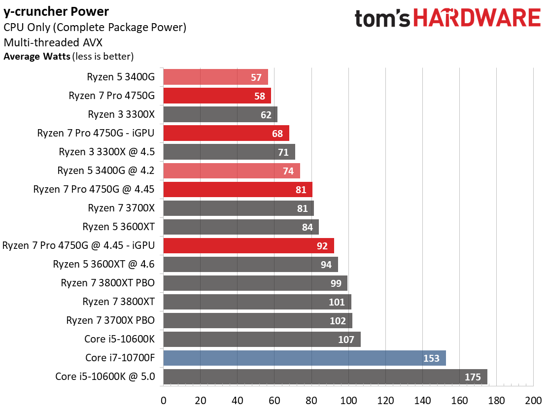
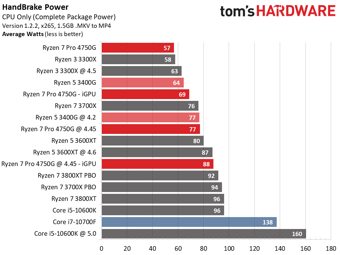
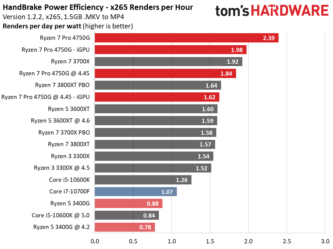
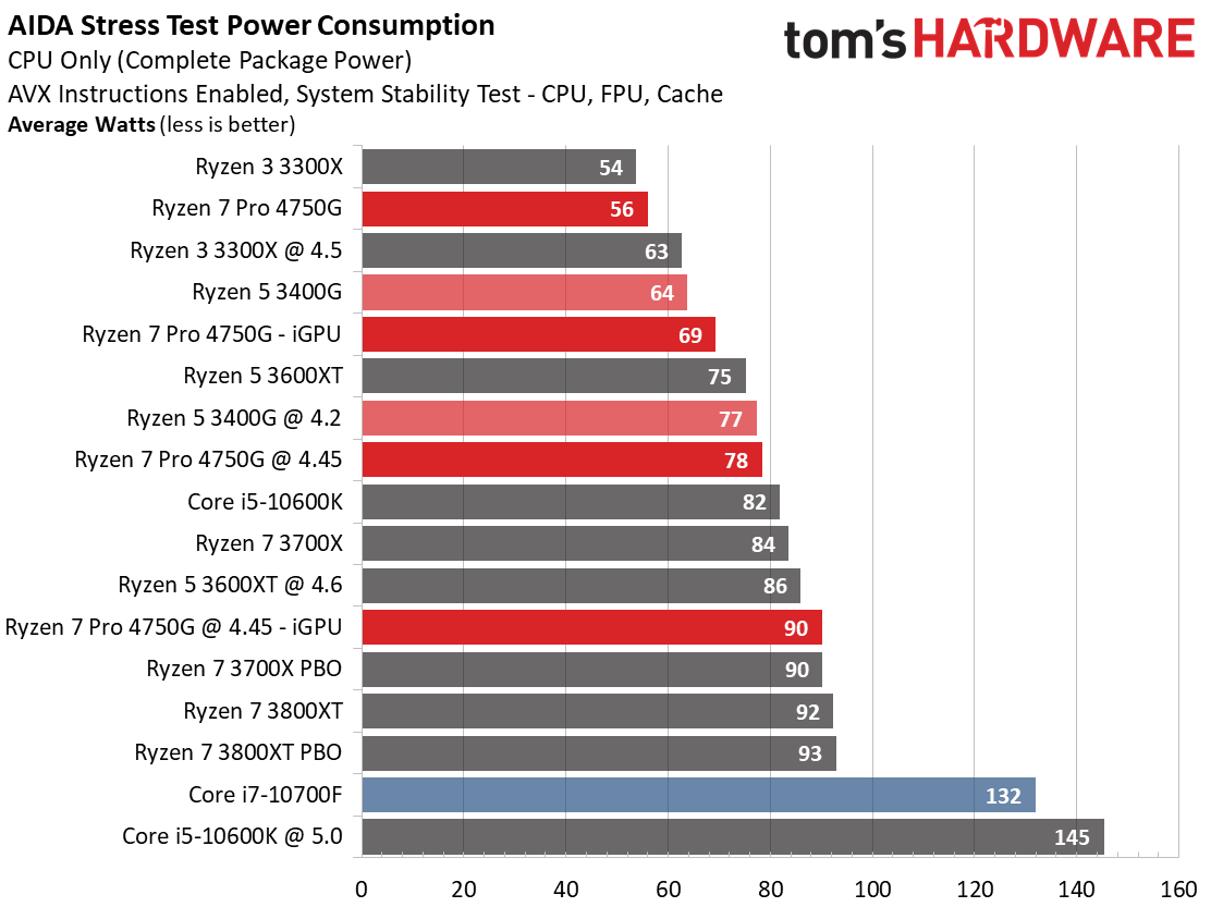
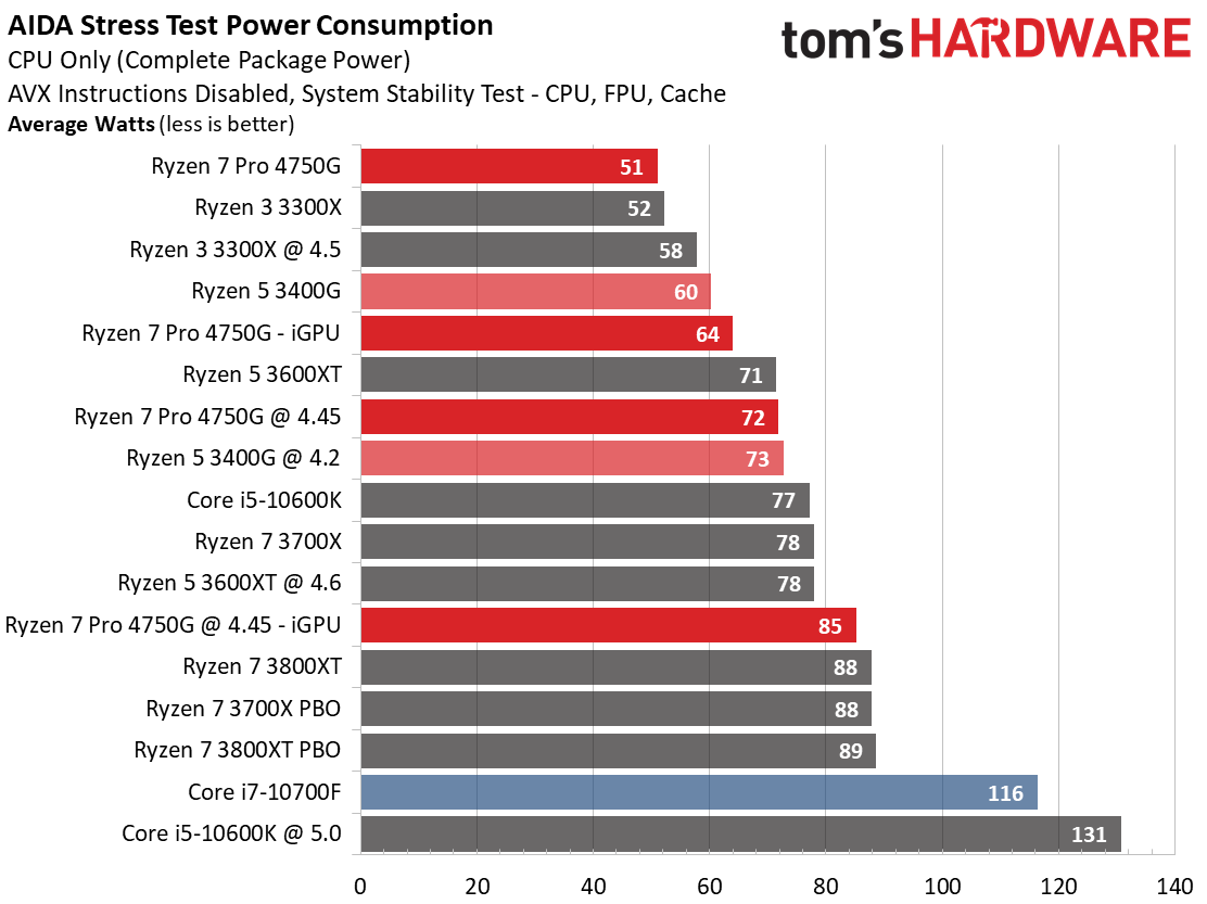
At stock settings with the discrete GPU, we logged an average of 58W of power consumption for the 4750G during the AVX-intensive multi-threaded y-cruncher workload. That's incredibly impressive given that the quad-core Ryzen 5 3400G only consumed 1W less — that means AMD has essentially doubled the core count within the same power envelope. We recorded 81W with the overclocked 4750G, and running the same test with the integrated graphics active yielded ~10W more power consumption for both configurations.
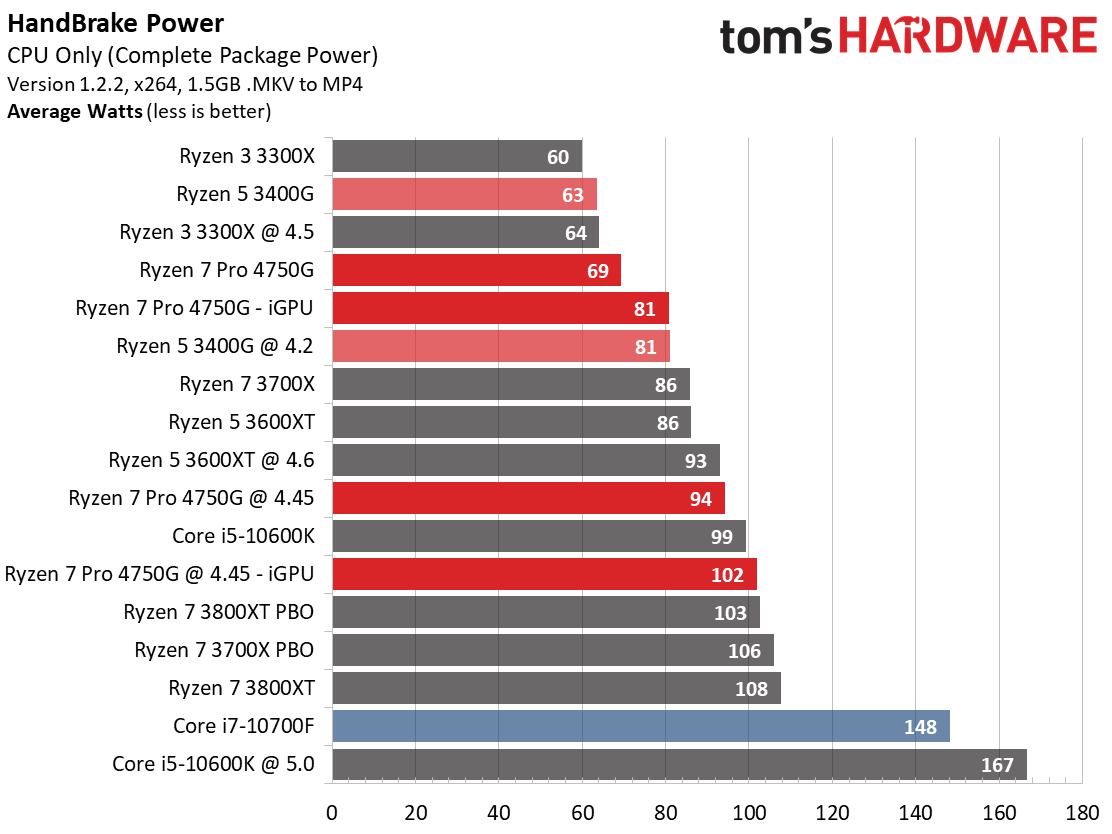
The 4750G reached 81W of power consumption during the x264 HandBrake render test (integrated graphics) and peaked at 102W after overclocking. That isn't bad at all, considering that the eight-core Core i7-10700F pulls 148W at stock settings (the chip isn't overclockable).
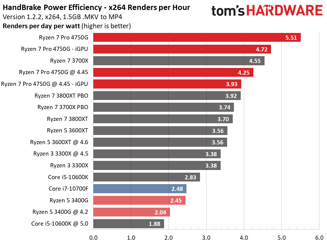
Flipping through to the HandBrake renders-per-hour charts show that Renoir sets the new bar for efficiency, both with and without the integrated graphics unit active.
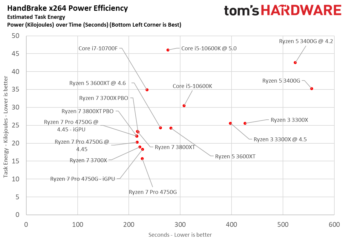
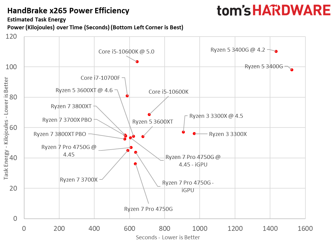
Here, we take a slightly different look at power consumption by calculating the cumulative amount of energy required to perform an x264 and x265 HandBrake workload, respectively. We plot this 'task energy' value in Kilojoules on the left side of the chart.
These workloads are comprised of a fixed amount of work, so we can plot the task energy against the time required to finish the job (bottom axis), thus generating a really useful power chart. Bear in mind that faster compute times, and lower task energy requirements, are ideal. That means processors that fall the closest to the bottom left corner of the chart are best.
The Ryzen 7 Pro 4750G falls in line with the other 7nm Ryzen processors, albeit lower (which is better) when the iGPU isn't active. This marks yet another solid performance from the 7nm Ryzen chips, and a quick glance at the far right upper corner finds the Ryzen 5 3400G chugging quite a bit more power for much lower performance. In terms of generational power efficiency improvements, Renoir takes a massive leap forward.
Get Tom's Hardware's best news and in-depth reviews, straight to your inbox.
As expected, the 7nm Ryzen 3000 processors continue to exhibit lower power draw and superior power efficiency compared to Intel's Core chips with the hyper-optimized, but old, 14nm process.
Ryzen 7 Pro 4750G Boost, Power and Thermals
Renoir adds some interesting caveats to our power testing, particularly in regard to how the integrated graphics impact both power consumption and CPU performance. First, we ran our standard frequency test for lightly-threaded workloads (methodology here) that steps through five iterations of the LAME encoder, then single-threaded POV-Ray and Cinebench runs, PCMark 10, GeekBench, and finally the VRMark Orange Room test. To keep the charts 'clean,' we only plot the maximum and minimum frequencies recorded on any one core during the test.
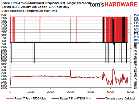
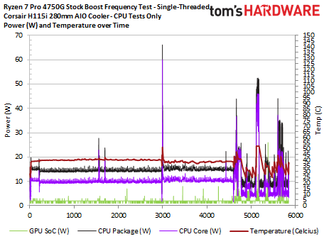
For this series of CPU-centric tests, we used the integrated graphics with the chip running on the ASUS B550-E gaming motherboard. The first slide shows that at least one core ran at 4.45 GHz, a slight increase over the rated 4.4 GHz boost, at nearly all times during our test. This is a lightly-threaded workload, so power and thermals are of little concern.
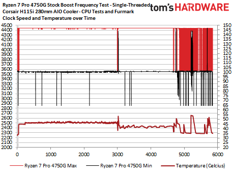
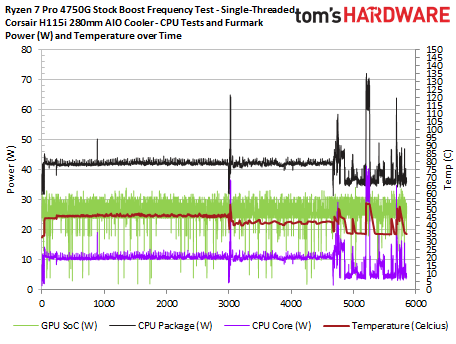
As outlined on the second slide, we kicked off a Furmark stress test to stress the graphics cores while we performed the same test. The intention here is to see if the increased thermal generation from the fully-loaded iGPU will impact peak frequencies in lightly-threaded workloads – and it didn't. The chip temperature jumped by roughly 5C, but the second chart shows that the chip still hit its boost frequency at nearly all times. That isn't too surprising; after all, these are lightly-threaded tests. We'll see a different result below in heavier multi-core workloads.
But first, flip over to the third slide. Here we can see the power consumption of the GPU cores, CPU cores, and total power consumption during our first test without Furmark. Here we can see the GPU cores sucking down ~5W during most of the test, while the lion's share of the total power consumption comes from the CPU cores.
The fourth slide shows the power consumption of the elements when we ran the test with Furmark actively hammering the GPU cores. The CPU core power consumption remains consistent with the first test, but the iGPU jumps to the 25W to 30W range. CPU performance isn't impacted, though – the 40W of total power consumption tells us that the chip still has plenty of headroom to AMD's 88W socket power limit (PPT) during stock operation. Let's see what it looks like when we try to break that limit.
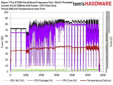
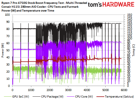
We turned the power up a notch with a string of real-world multi-core stress tests that includes the Corona ray-tracing benchmark, x265 HandBrake rendering tests, POV-Ray multi-threaded benchmarks, Cinebench R20 runs, and finally five iterations of the AVX-intensive threaded y-cruncher, all in rapid succession.
We're following the same test methodology – first a test with the graphics cores merely displaying the desktop during these CPU-centric tests, and then repeating the same test with Furmark hammering the graphics cores to full utilization. The goal is to see the power limits of the chip at stock settings, and how the processor balances power allocation between the CPU cores and GPU when it reaches the socket power limit.
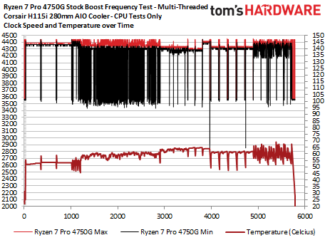
The first chart shows the chip chugging along through the workloads, with periods of scattered minimum frequency readings occurring during workloads that don't fully load all cores — like the HandBrake encoding tests from 1500~3000 seconds. The minimum and maximum frequencies converge during some portions of the run, indicating the all-core frequency when all cores are loaded. We see an all-core frequency of 4.4 GHz during non-AVX workloads, and 4.3 GHz during heavier AVX tests.
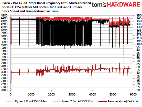
The second chart plots out the same test, but this time with the graphics cores fully stressed (and drawing power/generating heat) during the sequence. Here we see that all-core frequencies are markedly lower as we near the end of the test. These drops coincide with our runs of the AVX-heavy y-cruncher test.
Naturally, lower frequencies equate to lower performance. The third chart shows the power reading when the graphics engine was merely rendering the desktop. Here the CPU cores consumed roughly 80W of power during the heavier portions of the test, with the GPU cores contributing ~5W to 7W, thus pushing the chip to its 88W PPT limit. At that point, the chip isn't allowed to consume any more power, which becomes interesting when we hammer the graphics simultaneously.
The fourth chart, which plots the same series of tests with Furmark running, shows the graphics cores jump to ~20W to ~25W (~5W less than we recorded during the lightly-threaded tests), and the CPU cores downshift to 60W — that's 20W less than we recorded when the GPU was essentially at idle. Here the chip again never passes the 88W PPT limit, so it is doing its best to balance the limited power budget between both the CPU and GPU cores. However, the chip is measurably slower in both CPU and GPU workloads when both units are fully active/power constrained.
Granted, this is an extreme example of power balancing, but it does show that there can be a bit of a dynamic performance envelope during heavy usage. Where that lands is hard to determine for all workloads and use-cases, so we do our best to isolate our real-world testing on the following pages to the relevant compute units.
Let's see what it looks like when we overclock, which lets us blast past most of the limits.
Test Setup and Ryzen 7 Pro 4750G Overclocking
| Row 0 - Cell 0 | CPU Cores | Radeon RX Vega Graphics | Memory | Infinity Fabric (FCLK) |
| Ryzen 7 4750G Overclock | 4.45 GHz | 2400 MHz | DDR4-4000 | 2000 MHz |
AMD's auto-overclocking Precision Boost Overdrive (PBO) feature is available if you use an X- or B-series board, though you can unlock much higher performance through manual tuning. You can't install Ryzen Master on a system with the Renoir APUs. Still, if you have already installed Ryzen Master with a 'standard' Ryzen processor, it will work with the Pro models – the current public version of the software just blocks a fresh install.
Manually overclocking Renoir is fun, but challenging. The chip responds readily to voltage — we dialed in a solid 4.45 GHz all-core overclock by simply bumping up the vCore to 1.36V and adjusting the multiplier.
Overclocking Renoir's memory was a bit more involved, but we began by disabling AMD's system memory encryption (TSME). This feature only comes on the Pro chips, and it's enabled by default. Unfortunately, it creates overhead, so our stock memory latency dropped from 80.2ns to 72.2ns just by disabling the feature. That's a nice gain for simply flipping a switch. This really is the only performance-impacting difference between the Pro and non-Pro models. To simulate what you could expect from the consumer chips, we conducted all of our tests on the following pages with TSME disabled.
We're told that good Renoir chips can support a fabric clock (FCLK) of 2300 MHz, but we dialed in a setting of 2000 MHz so we could mix in CPU and iGPU overclocks as well. (You can push the FCLK higher if you use a discrete GPU rather than the iGPU – this reduces traffic and contention on the Infinity Fabric, which leads to lower latency). The 2000 MHz is much better than the typical 1900~1933 MHz FCLK tolerated by most Matisse processors.
Setting the FCLK to 2000 MHz allowed us to dial in an easy DDR4-4000 at a 1:1 FCLK/memory clock ratio. This 'coupled mode' is the sweet spot for memory latency on AMD's Zen 2 platforms, but dialing in a 2300 MHz FCLK will allow you to reach DDR4-4600 while still in coupled mode. We set our memory to 16-18-18-56 timings, yielding 67.7ns of memory latency. However, there have been plenty of examples of enthusiasts hitting ~40ns with optimal sub-timings and a discrete GPU, so there's plenty of room for improvement for experienced tweakers.
To maintain consistency in our test pool, we used the 4.45 GHz CPU overclock paired with DDR4-4000 memory for our application testing on the MSI X570 Godlike and a discrete GPU, but left the iGPU st stock settings for those tests.
We added an iGPU overclock for our integrated graphics gaming tests on the ASUS B550-E gaming. Most 'good' Ryzen 7 Renoir chips can hit ~2500 MHz on the iGPU, but ours topped out at a stable 2400 MHz – artifacting and other errata took hold with higher frequencies. We dialed in 1.32V on the iGPU, then adjusted SoC voltage to 1.3V and VDDP to 1.3V to ensure that the CPU, GPU, and memory all ran stably while simultaneously overclocked.
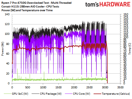
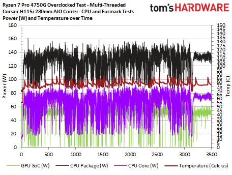
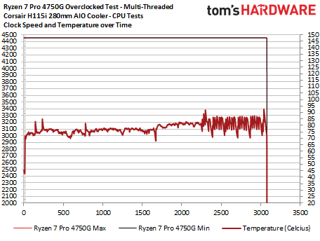
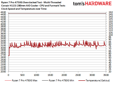
The results of our efforts were pretty satisfying, and Renoir's soldered die helps with temperatures. Here you can see two tests that follow our test methodology outlined in the boost testing above. The Ryzen 7 Pro 4750G is running with DDR4-4000 in coupled mode along with overclocked CPU and GPU Cores (4.45 GHz and 2400 MHz, respectively) on the B550-E Gaming motherboard.
The first slide shows power consumption during our string of multi-threaded applications, but with the iGPU merely displaying the desktop. Here the graphics pulls ~9W, while the CPU cores are free to roam well above the 88W PPT power limit, which has now been removed. Total package power peaks at 120W during the test, leading to a peak of 92C for a brief moment. Temperatures largely hovered in the 80C~85C range during the most demanding portions of the test. Still, it's worth pointing out that we're using a 280mm Corsair H115i AIO with its fans cranking away at full blast: You can, and likely will, become thermally constrained during overclocking with lesser coolers. The Corsair H115i, and equivalent coolers, are pricey for this class of chip, so keep that in mind.
The second chart shows the results when we kick on the Furmark stress test during the same series of tests. Here the total package power peaks around 160W, but mostly hovers in the 140W range. As expected, iGPU power consumption shoots up to ~60W, but the CPU power consumption drops from the 120W in the previous test to 65W~80W. Thermals remained comfortably below 85C during this run, so that isn't a limiting factor. A quick glance at Ryzen Master revealed that we had pegged the Electrical Design Current (EDC) limit while PPT and EDT still had plenty of room to maneuver. Our initial assessment is that the power delivery subsystem on the B550E is holding us back from squeezing out a few more watts of performance, but it's also possible that we're just hitting the limit of the chip. This is an extreme corner case, for sure, and it will be interesting to see if we can squeeze out some more headroom on other B550 motherboards.
| AMD Socket AM4 (B550) | Ryzen 7 Pro 4750G |
| Row 1 - Cell 0 | iGPU - ASUS ROG STRIX B550E Gaming |
| Row 2 - Cell 0 | 2X8 GB G.Skill Trident Z Royal DDR4-3600 - Stock: DDR4-3200, OC: DDR4-4000 |
| AMD Socket AM4 (B450) | Ryzen 5 3400G |
| Row 4 - Cell 0 | iGPU - ASUS Tuf B450M-Plus Gaming |
| Row 5 - Cell 0 | 2X8 GB G.Skill Trident Z Royal DDR4-3600 - Stock: DDR4-3200, OC: DDR4-4000 |
| Intel Socket 1200 (Z490) | Core i7-10700K, i7-10700F, Core i5-10600K |
| Row 7 - Cell 0 | Apps, dGPU, iGPU - Gigabyte Aorus Z490 Master |
| Row 8 - Cell 0 | 2x 8GB G.Skill FlareX DDR4-3200 - Stock: DDR4-2933, OC: DDR4-3600 |
| AMD Socket AM4 (X570) | AMD Ryzen 7 4750G (Apps/dGPU), Ryzen 7 3700X, 3800XT, Ryzen 5 3600XT, 3400G, Ryzen 3 3300X |
| Apps and dGPU- MSI MEG X570 Godlike | |
| Row 11 - Cell 0 | 2x 8GB G.Skill FlareX DDR4-3200 - Stock: DDR4-3200, OC: DDR4-3600 |
| All Systems | Nvidia GeForce RTX 2080 Ti |
| 2TB Intel DC4510 SSD | |
| EVGA Supernova 1600 T2, 1600W | |
| Row 15 - Cell 0 | Open Benchtable |
| Windows 10 Pro (1903 - All Updates) | |
| Cooling | Corsair H115i |
MORE: Best CPUs
MORE: Intel and AMD Processor Hierarchy Comparisons
MORE: All CPUs Content
Current page: AMD Ryzen 7 4750G Boost, Thermals, Overclocking, Power Consumption
Prev Page Zen 2 and 7nm APUs Land on the Desktop Next Page AMD Ryzen 7 Pro 4750G Integrated Vega Graphics Gaming Benchmarks
Paul Alcorn is the Editor-in-Chief for Tom's Hardware US. He also writes news and reviews on CPUs, storage, and enterprise hardware.
-
mdd1963 I expected /hoped for a bit more than bumping FPS in games up only 10-15% compared to the 3400G.... (Apparently I will not be happy until they can match GTX1060-level of performance into the APU)Reply -
neojack impressive results ! this APU is more powerfull than my 2700x in raw power, AND has an igpu about equal to a gtx 1050Reply -
JarredWaltonGPU Reply
It's a bit weird, because the memory bandwidth is lower but all system RAM can be treated as shared VRAM, so you can sometimes run higher settings with less performance problems on in integrated Vega 8 GPU than on a dedicated GPU. But in general, Vega 8 for Renoir is roughly equal to an RX 560, which is basically equal to a GTX 1050.Gurg said:Curious as to which discrete GPU the iGPU is the equivalent.
In a lot of cases, the 1050 is still 25% faster, though. For example, Far Cry 5 1080p normal settings, I got 43 fps, Shadow of the Tomb Raider 1080p Medium I got 39 fps, and Strange Brigade 1080p medium I got 72 fps. That means the GTX 1050 beat the integrated 4750G's Vega 8 Graphics, even when the latter was overclocked. And the GTX 1050 is a pretty slow GPU by today's standards -- the GTX 1650 Super is over twice as fast as the GTX 1050. -
Gurg Reply
Thanks for the reply. It seems like a CPU/iGPU for a $1,000 laptop without a discrete GPU.JarredWaltonGPU said:It's a bit weird, because the memory bandwidth is lower but all system RAM can be treated as shared VRAM, so you can sometimes run higher settings with less performance problems on in integrated Vega 8 GPU than on a dedicated GPU. But in general, Vega 8 for Renoir is roughly equal to an RX 560, which is basically equal to a GTX 1050.
In a lot of cases, the 1050 is still 25% faster, though. For example, Far Cry 5 1080p normal settings, I got 43 fps, Shadow of the Tomb Raider 1080p Medium I got 39 fps, and Strange Brigade 1080p medium I got 72 fps. That means the GTX 1050 beat the integrated 4750G's Vega 8 Graphics, even when the latter was overclocked. And the GTX 1050 is a pretty slow GPU by today's standards -- the GTX 1650 Super is over twice as fast as the GTX 1050. -
Neilbob Replynofanneeded said:"Useless"
no 4th GEN PCIe means no one will buy it.
I agree. This is why Intel is unable to sell a single CPU! A computer without 4th GEN PCIe capability might as well be a brick, right?
(Sarcasm, just in case there's doubt) -
nofanneeded ReplyNeilbob said:I agree. This is why Intel is unable to sell a single CPU! A computer without 4th GEN PCIe capability might as well be a brick, right?
(Sarcasm, just in case there's doubt)
At least intel offers 16 lanes with their CPU . This chips only offers 8 lanes Gen3 .. useless. -
Neilbob Replynofanneeded said:At least intel offers 16 lanes with their CPU . This chips only offers 8 lanes Gen3 .. useless.
I would say 'limiting' rather than useless. Especially seeing as these APUs are intended for an OEM market that in all likelihood won't be pairing them with anything more than a mid-range GPU (that's what the Ryzen 3000 series is for).
Who's to say that more lanes won't be exposed if/when AMD release these for the DIY user base?
Of course, this is just pure speculation from me. Already got my 3600 so I'm all set either way (y)
Edit: So there actually are 16 lanes (which I missed in the review) so above posts turn out to be irrelevant.
