Why you can trust Tom's Hardware
AMD Zen 3 Ryzen 5000 Series Microarchitecture — The Quick Take
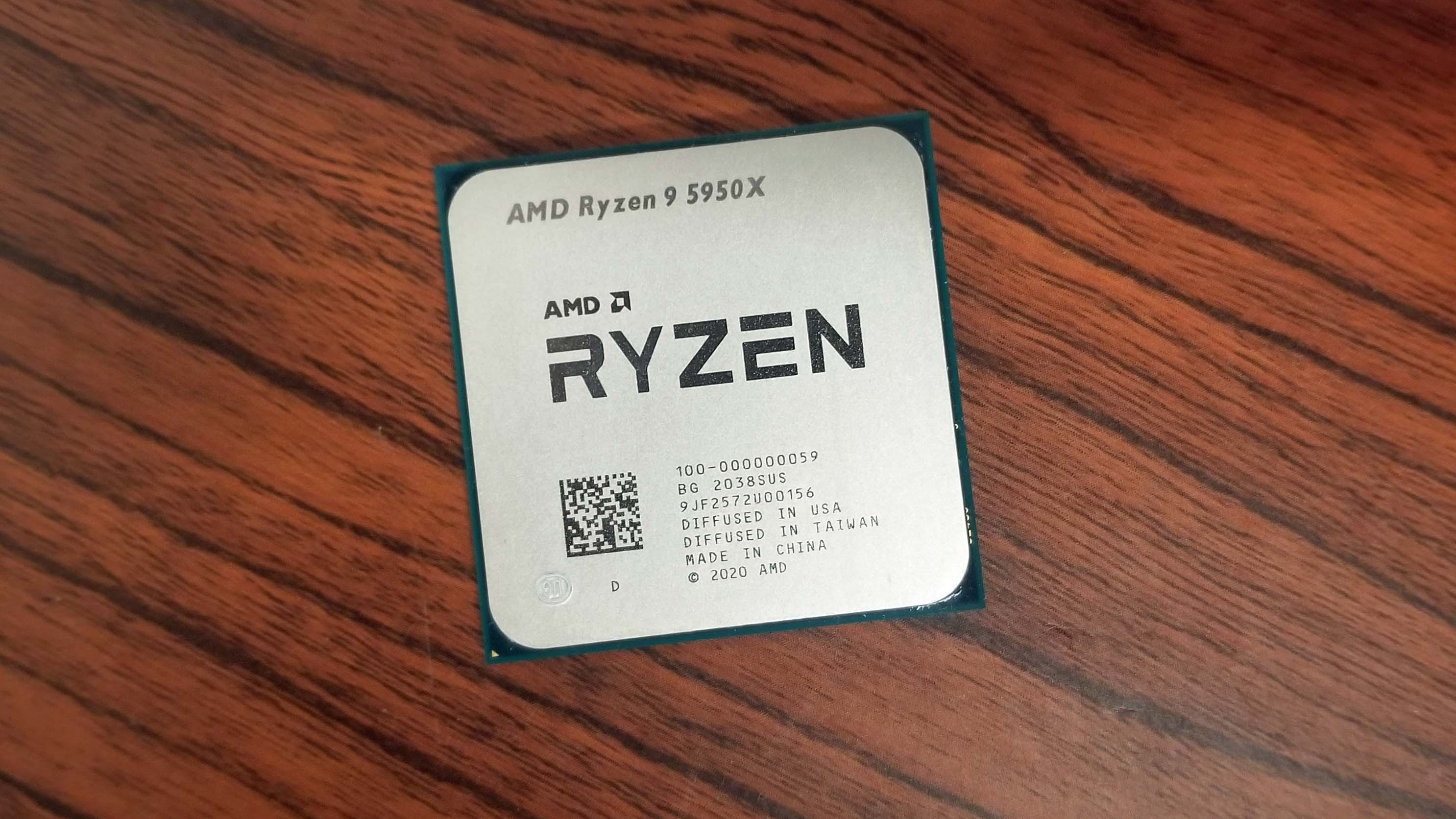
AMD's 19% IPC increase is the big headline feature of the Zen 3 microarchitecture, but it is especially impressive considering that it leveraged its existing Ryzen SoC to accomplish the feat. In fact, the base SoC is identical to the Ryzen 3000 processors: Zen 3 uses the same 12nm I/O Die (IOD) paired with either one or two 8-core chiplets (CCD) in an MCM (Multi-Chip Module) configuration. The IOD still contains the same memory controllers, PCIe, and other interfaces that connect the SoC to the outside world. Just like with the Matisse chips, the IOD measures ~125mm^2 and has 2.09 billion transistors.
The chiplets have been redesigned, however, and now measure ~80.7mm^2 and have 4.15 billion transistors. That's slightly larger than Zen 2's CCDs with ~74mm^2 of silicon and 3.9 billion transistors.
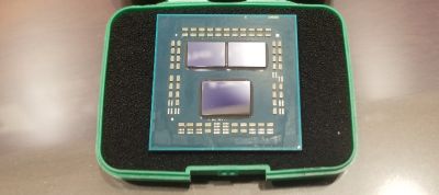
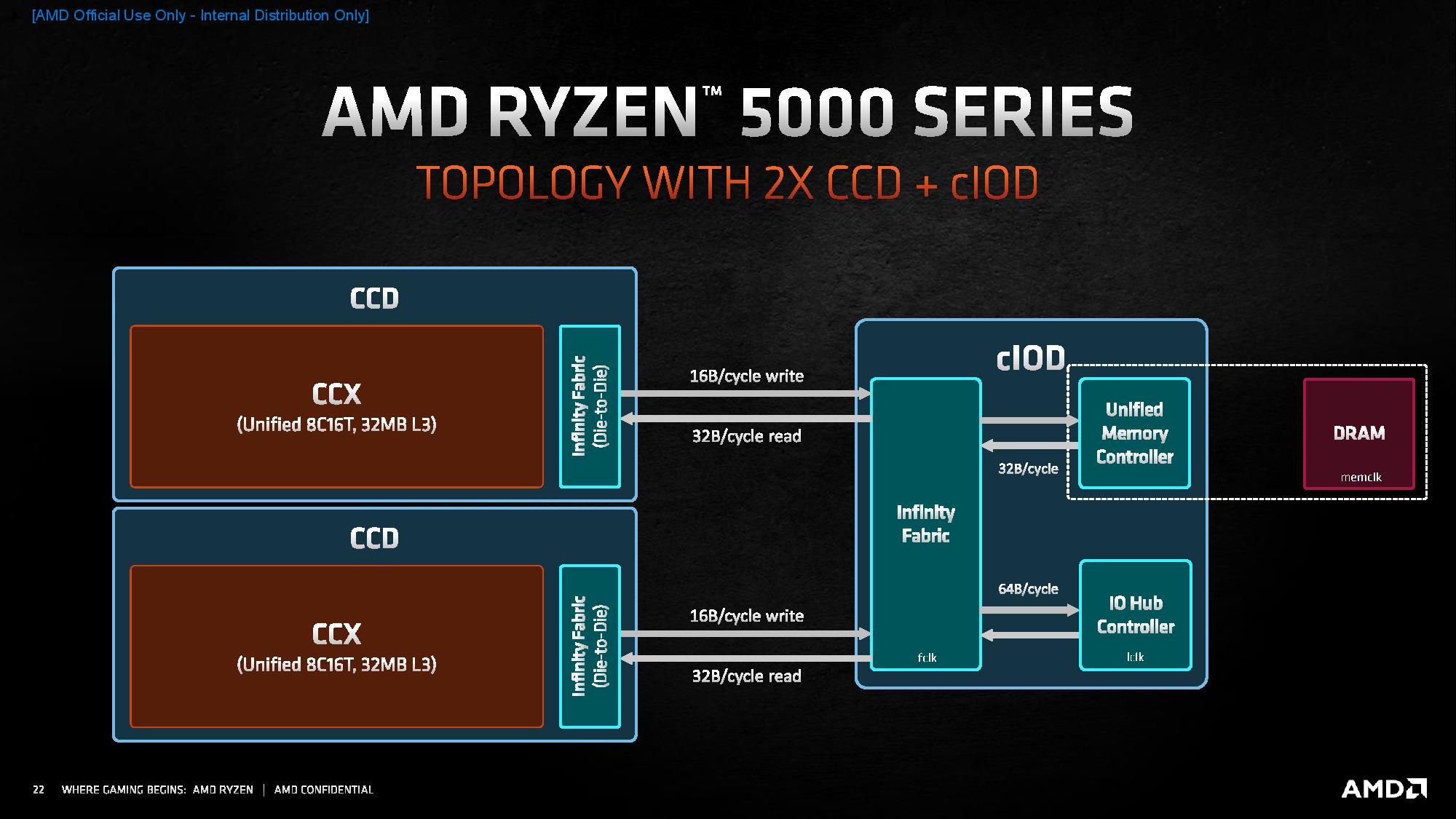
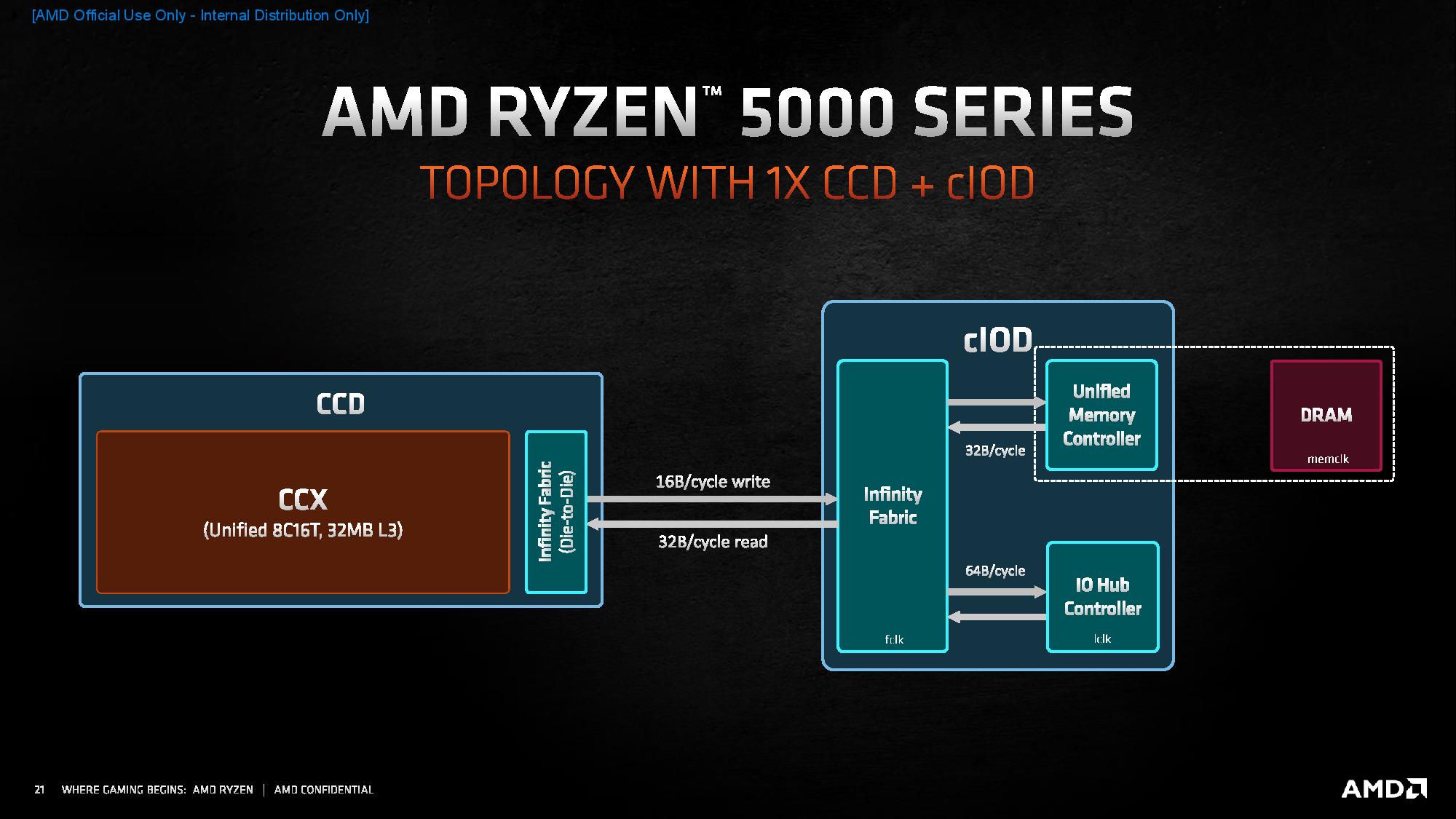
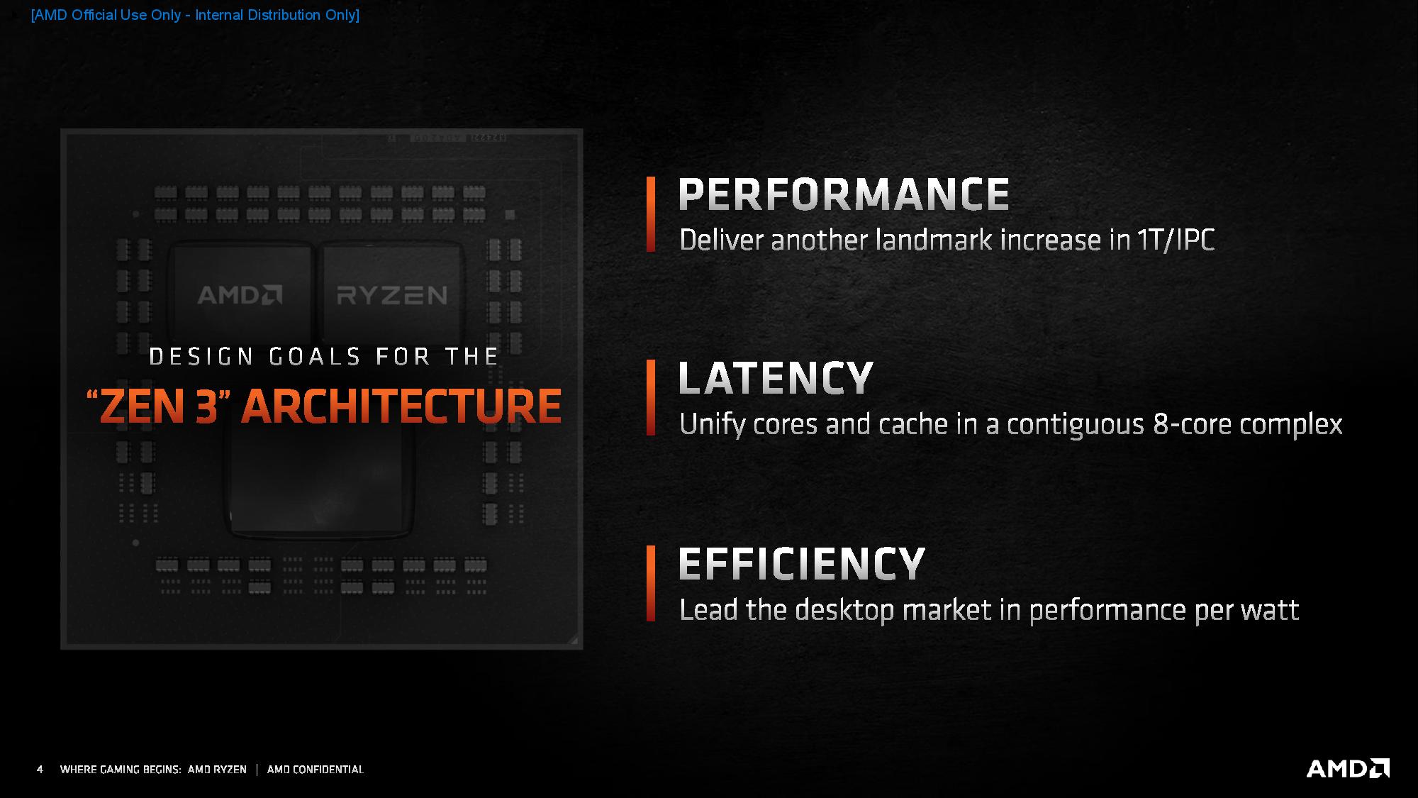
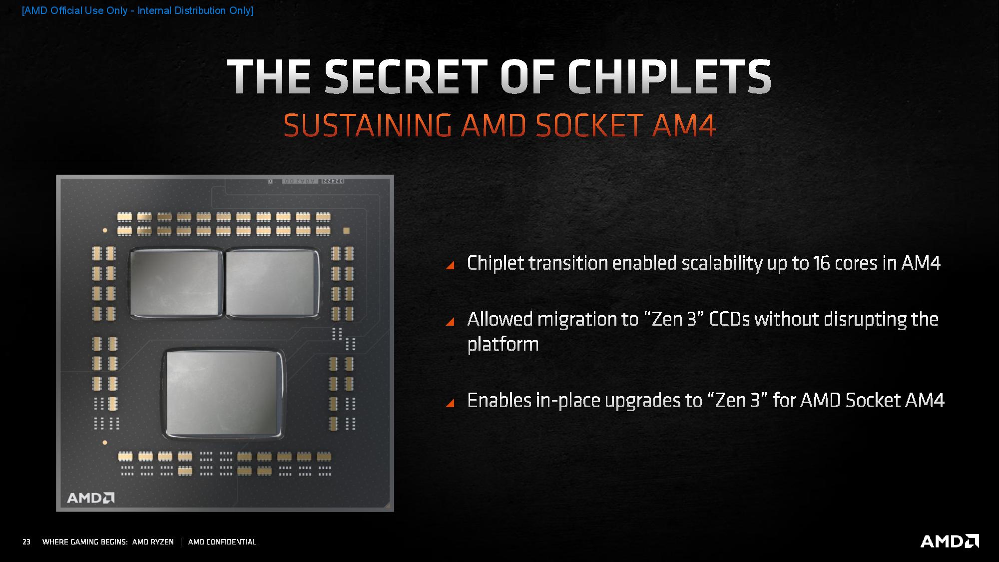
Just like the previous-gen Ryzen CPUs, processors with six or eight cores come with one compute chiplet, while CPUs with 12 or 16 cores come with two chiplets. AMD also used all of the existing SoC wire routing and packaging to maintain compatibility with the AM4 socket. As shown in the album above, the Infinity Fabric connections between the IOD and compute chiplets (CCD) remain the same and communicate at 32 Bytes-per-cycle for reads and 16B/cycle for writes. Even though these connections remain at the same speed as the previous-gen chips, the redesigned compute chiplets significantly reduce the amount of traffic that flows over the interface.
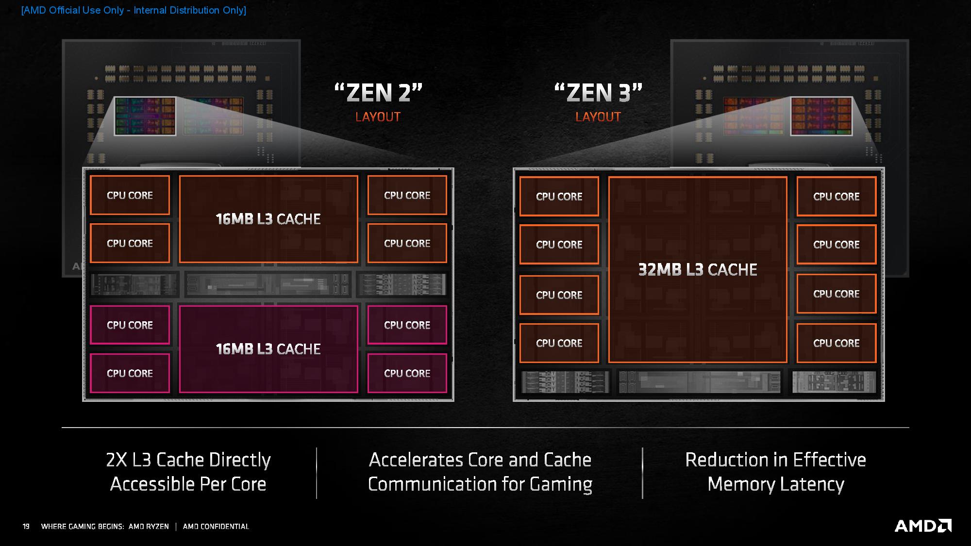
In the Zen 2 architecture (left), each Zen compute chiplet (CCD) contained two four-core clusters (CCXes) with access to an isolated 16MB slice of L3 cache. So, while the entire chiplet contained 32MB of cache, not all cores had direct access to all of the cache in the chiplet.
To access an adjacent slice of L3 cache, a core had to communicate with the other quad-core cluster by traversing the Infinity Fabric to the I/O die. The I/O die then routed the communication to the cache in the second quad-core cluster, even though it was contained within the same chiplet. To complete the transfer, the data had to travel back over the fabric to the I/O die, and then back into the adjacent quad-core cluster.
Each chiplet now contains one large unified 32MB slice of L3 cache, and all eight cores within the chiplet have full access to the shared cache. This improves not only core-to-cache latency but also core-to-core latency within the chiplet. AMD has also updated the CCD's core-to-core and cache interconnect to a ring topology.
While all eight cores can access the L3 cache within a single compute chiplet, in a dual-chiplet Zen 3 chip, there will be times that the cores will have to communicate with the other chiplet and its L3 cache. In those cases, the communications will still have to traverse the Infinity Fabric via signals routed through the I/O die.
Get Tom's Hardware's best news and in-depth reviews, straight to your inbox.
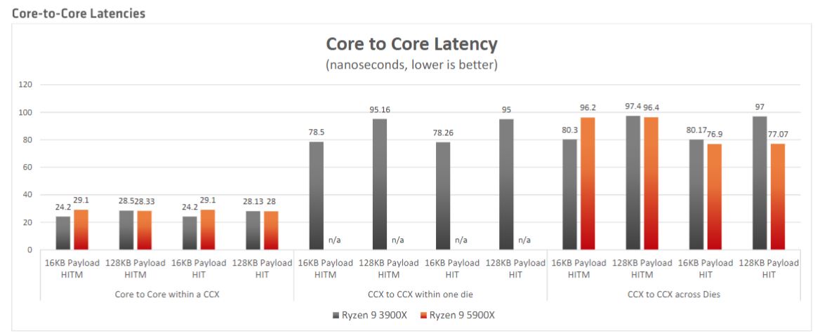
Still, because an entire layer of external communication between the two four-core clusters inside each chiplet has been removed (as seen in the center of the chart above), the Infinity Fabric will naturally have far less traffic. This results in less contention on the fabric, thus simplifying scheduling and routing, and it could also increase the amount of available bandwidth for this type of traffic. All of these factors will result in faster transfers (i.e., lower latency) communication between the two eight-core chiplets, and it possibly removes some of the overhead on the I/O die, too.
These enhancements are important because games rely heavily on the memory subsystem, both on-die cache and main memory (DDR4). A larger pool of cache resources keeps more data closer to the cores, thus requiring fewer high-latency accesses to the main memory. Additionally, lower cache latency can reduce the amount of time a core communicates with the L3 cache. This new design will tremendously benefit latency-sensitive applications, like games — particularly if they have a dominant thread that accesses cache heavily (which is common).
However, the larger L3 cache does come with an increase in L3 latency to the tune of seven additional cycles.
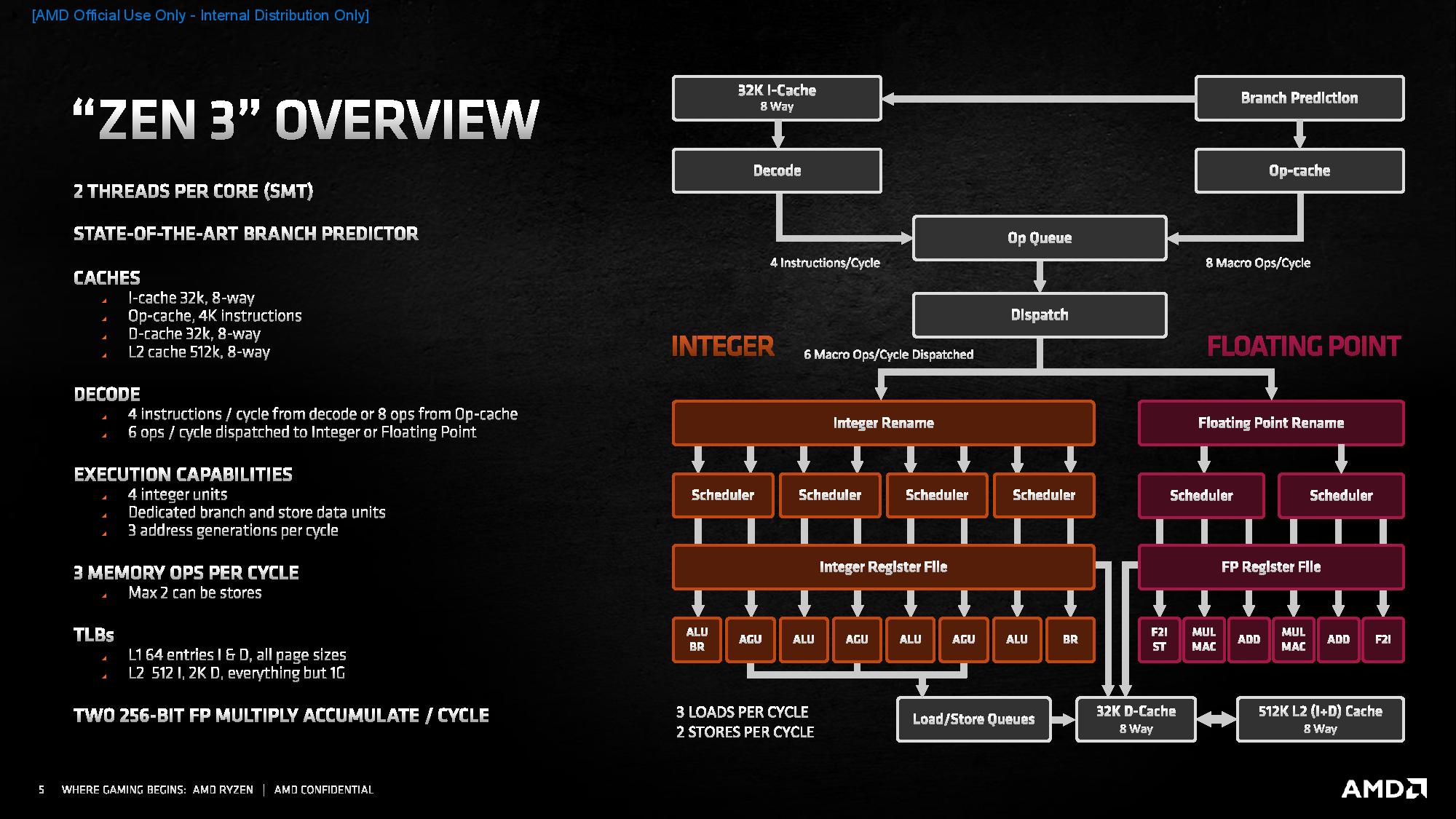
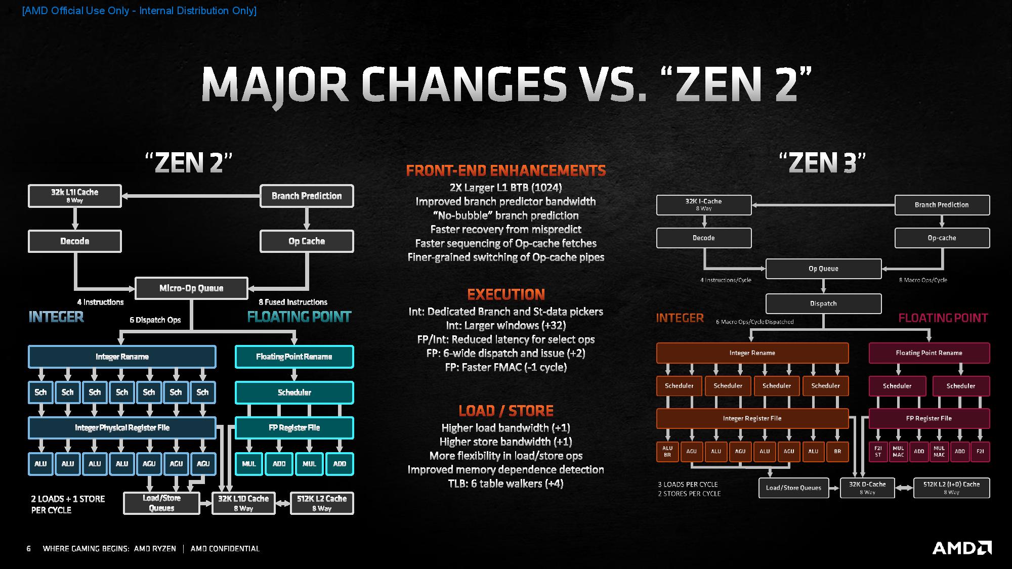
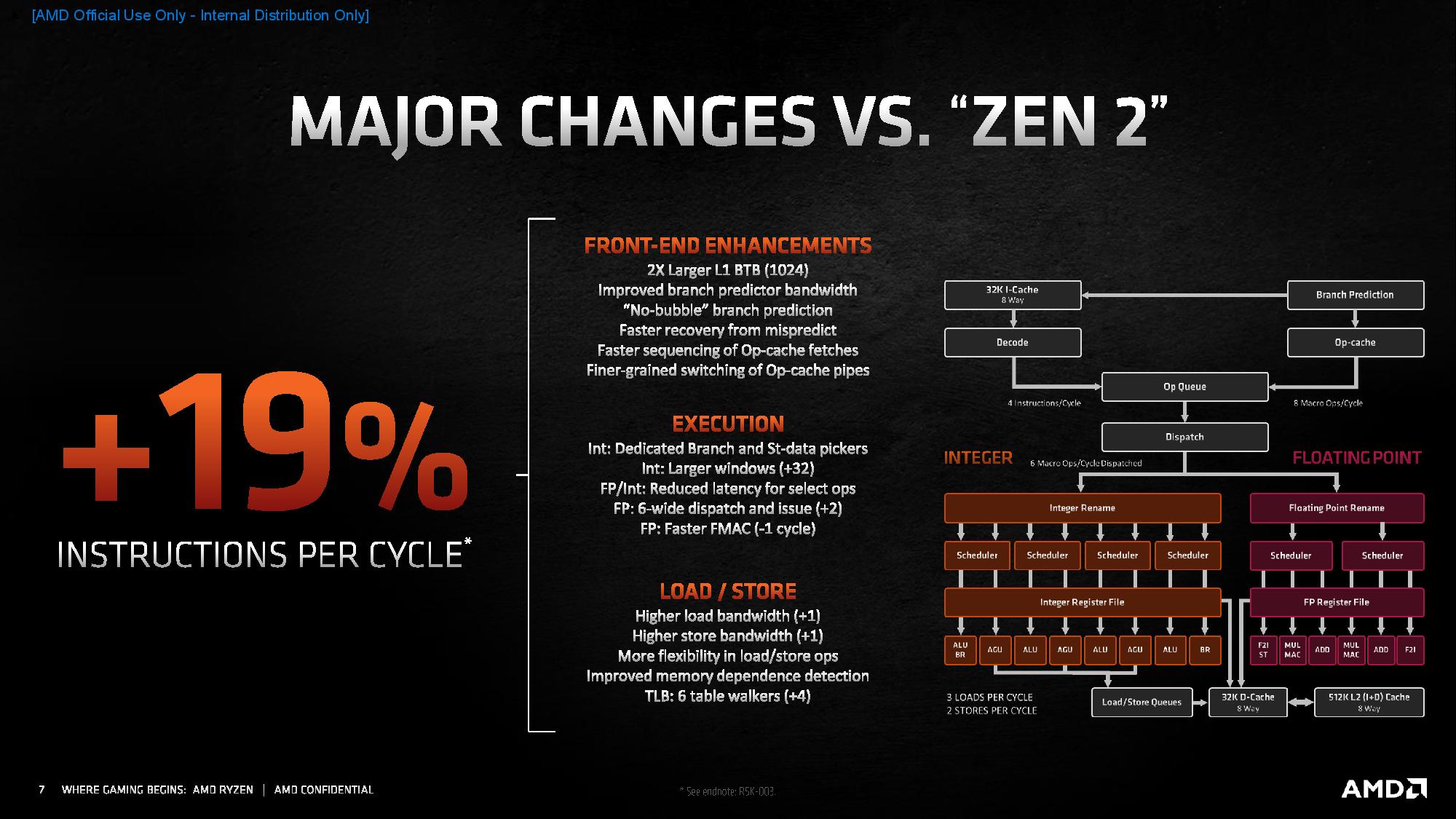
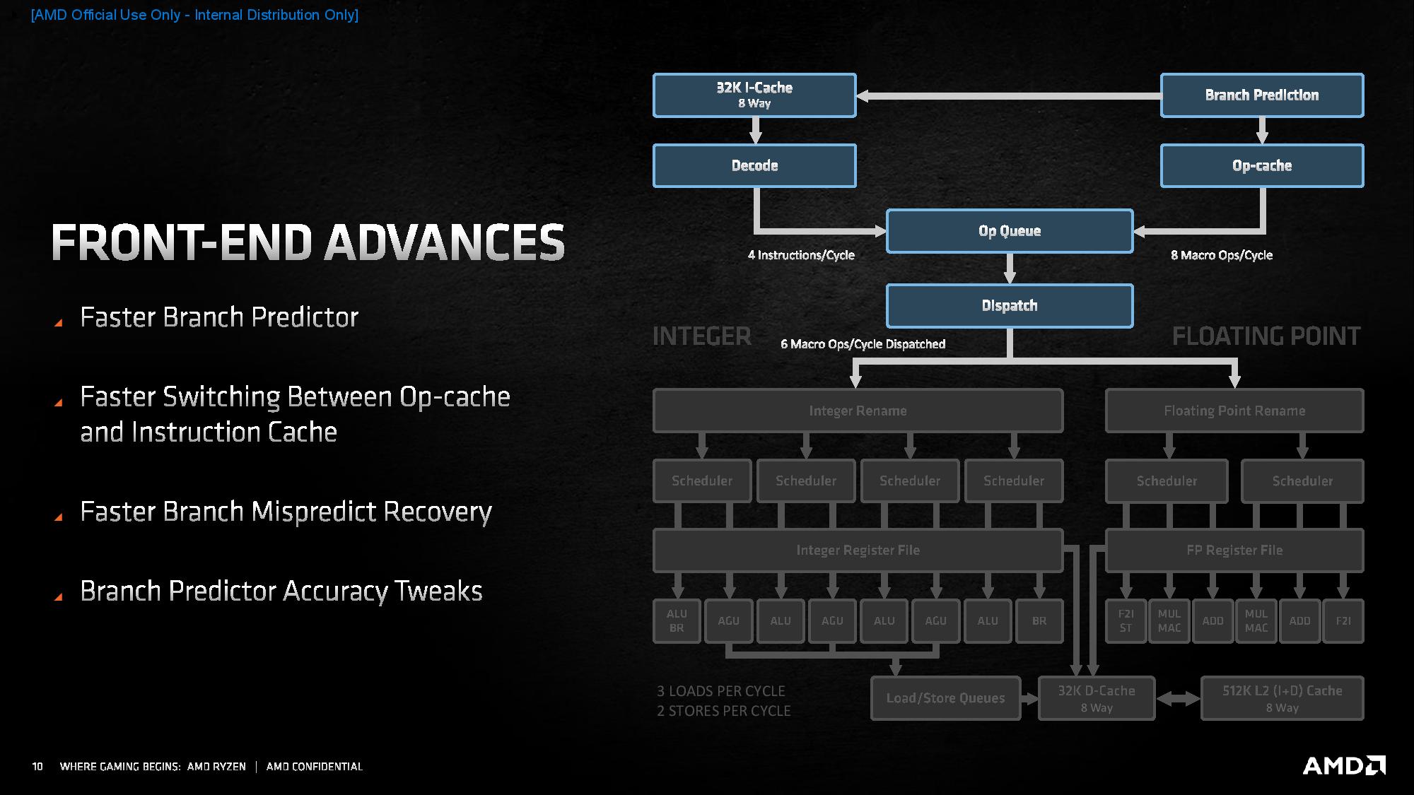
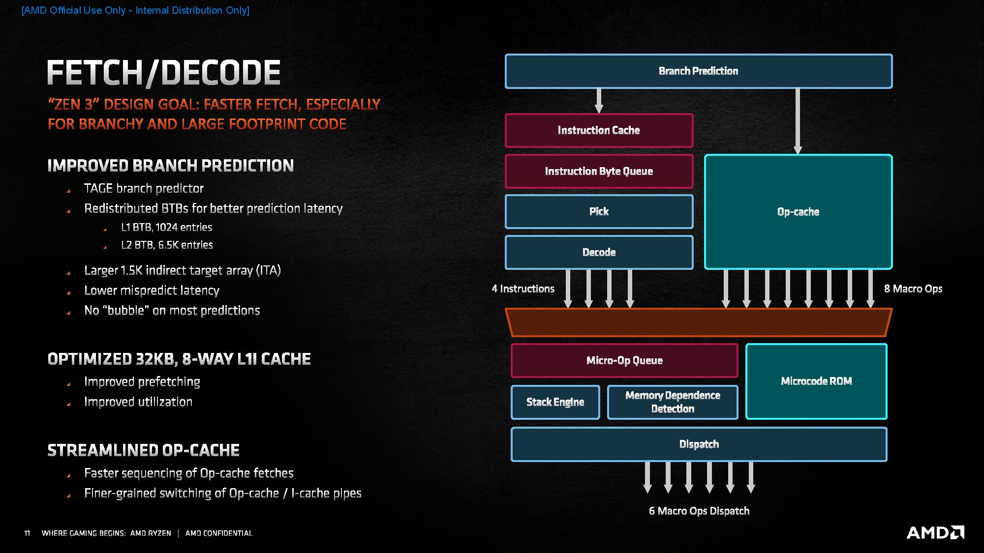
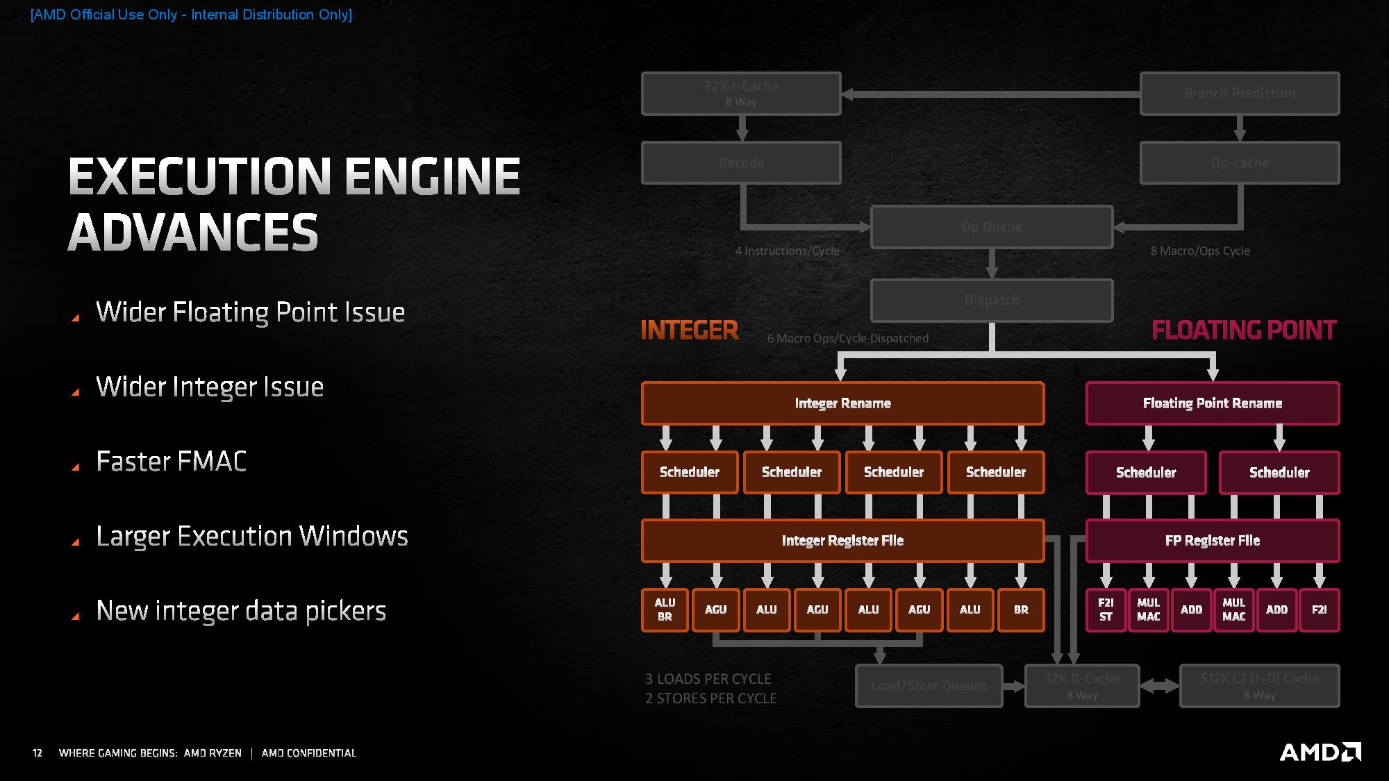
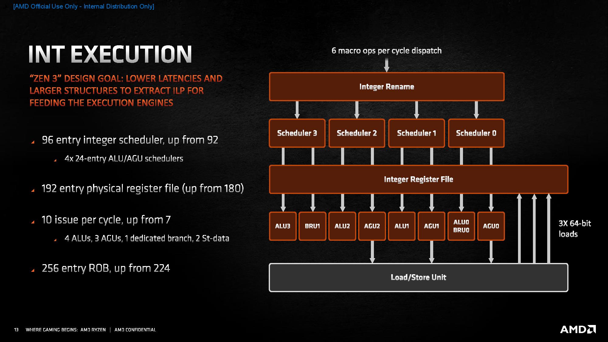
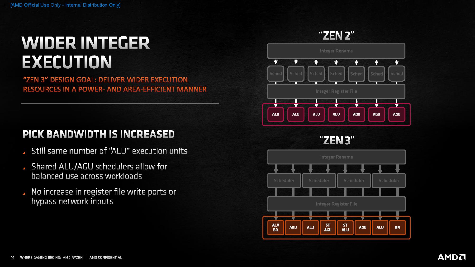
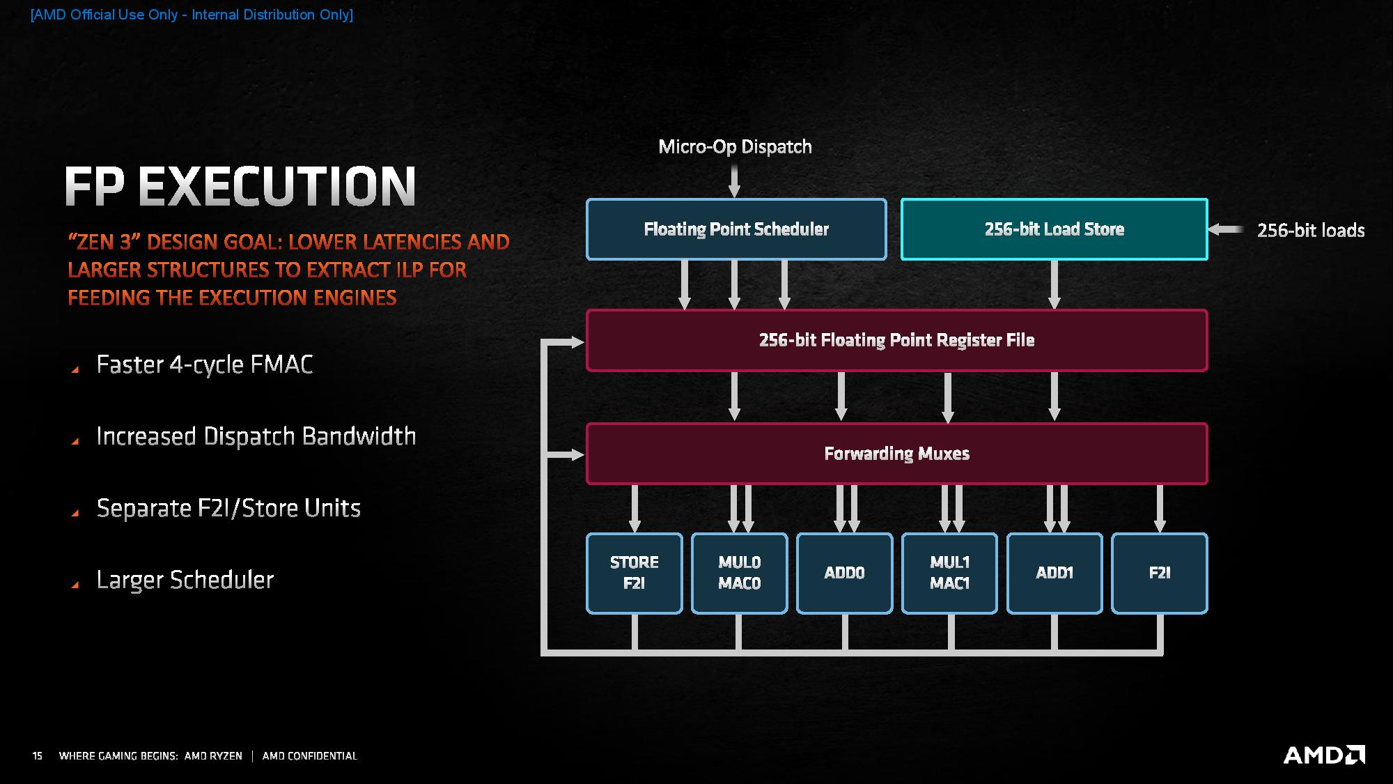
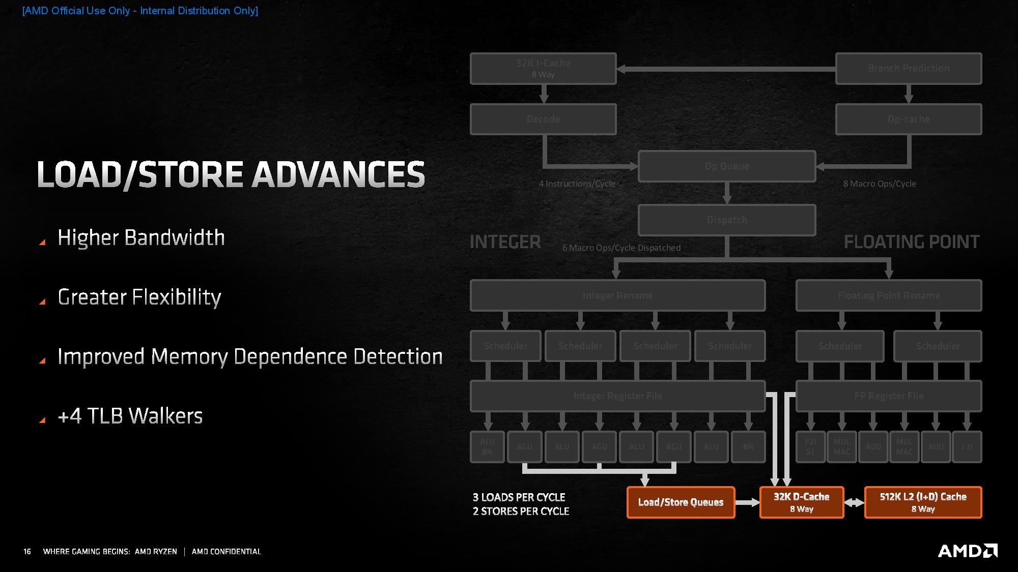
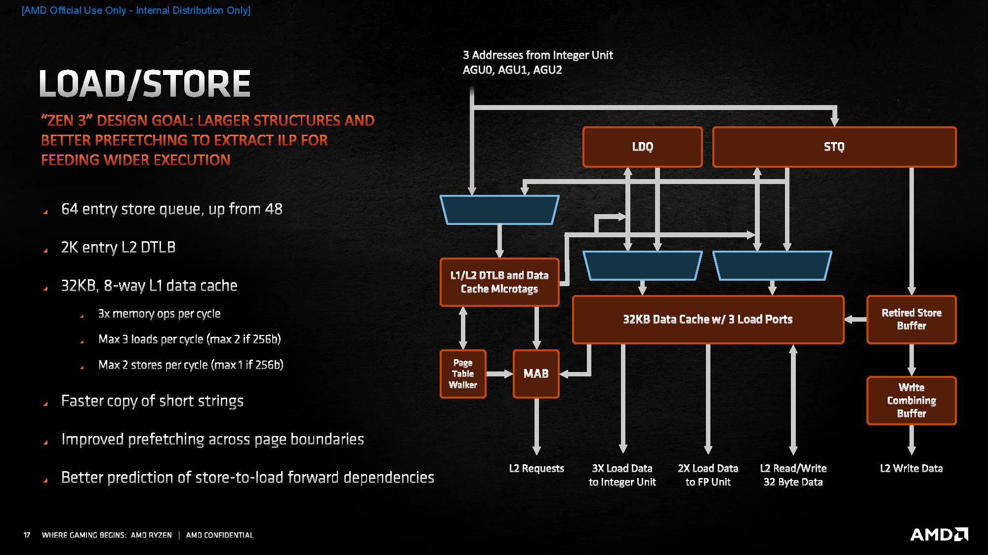
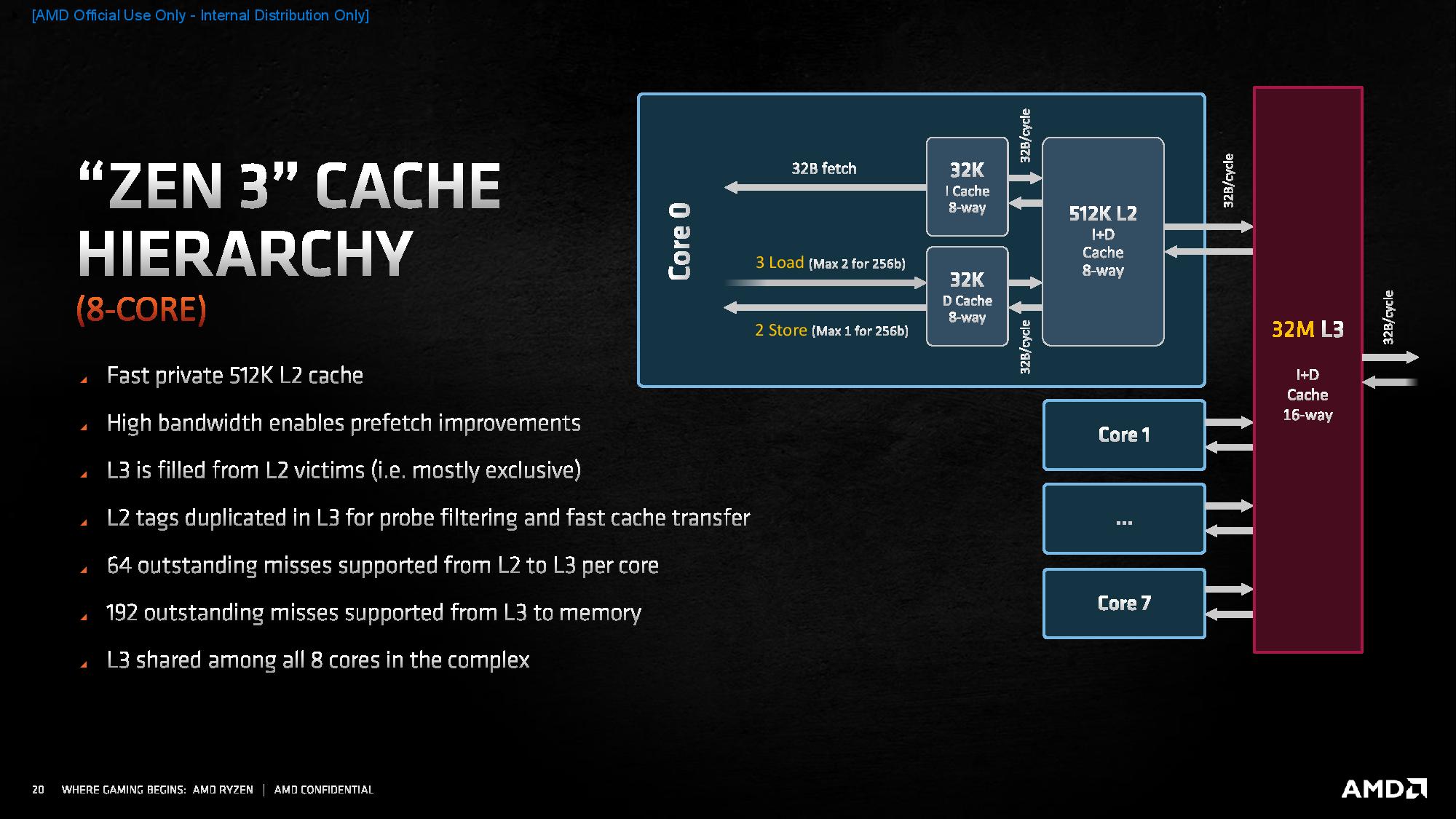
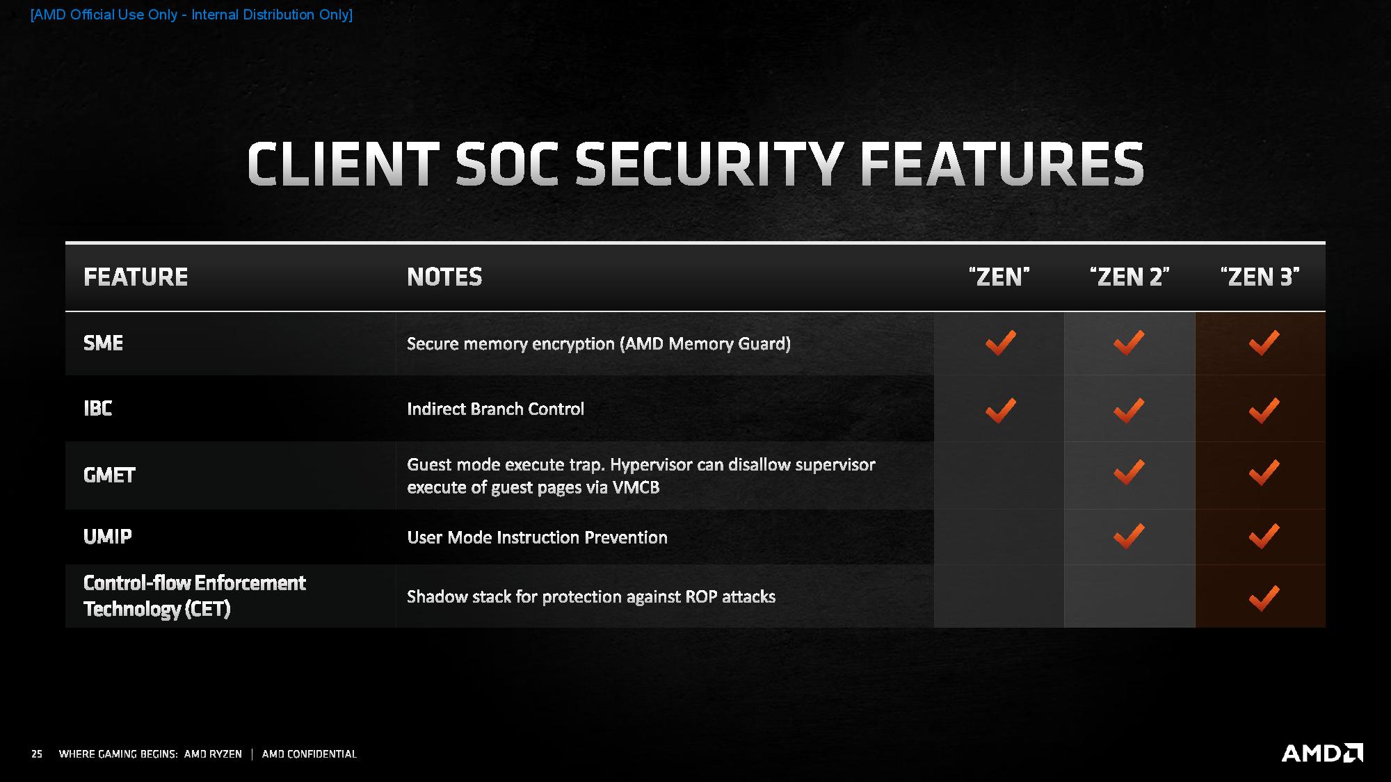
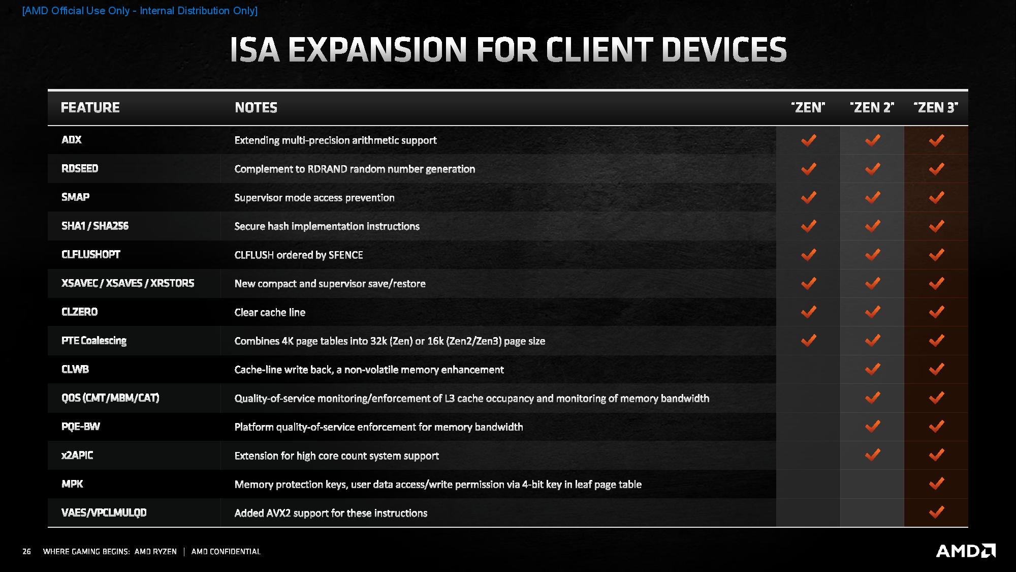
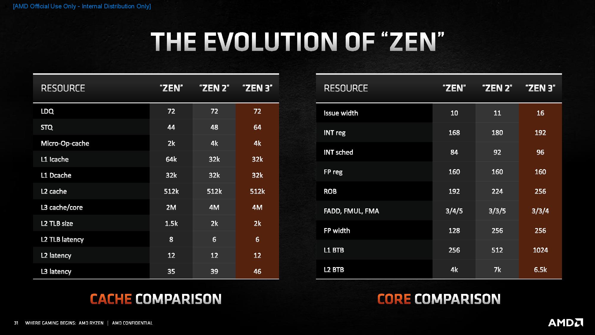
Here's AMD's high-level bullet point list of improvements to the Zen 3 microarchitecture:
- Front-end enhancements:
- Major Design Goal: Faster fetching, especially for branchy and large-footprint code
- L1 branch target buffer (BTB) doubled to 1024 entries for better prediction latency
- Improved branch predictor bandwidth
- Faster recovery from misprediction
- "No Bubble" prediction to make back-to-back predictions faster and better handle branchy code
- Faster sequencing of op-cache fetches
- Finer granularity in switching of op-cache pipes
- Execution Engines:
- Major Design Goal: Reduce latency and enlarge to extract higher instruction-level parallelism (ILP)
- New dedicated branch and st-pickers for integer, now at 10 issues per cycle (+3 vs. Zen 2)
- Larger integer window at +32 vs Zen 2
- Reduced latency for select float and integer operations
- Floating point has increased bandwidth by +2 for a total of 6-wide dispatch and issue
- Floating point FMAC is now one cycle faster
- Load/Store:
- Major Design Goal: Larger structures and better prefetching — enhance execution engine bandwidth
- Overall higher bandwidth to feed larger/faster execution resources
- Higher load and store bandwidth vs. Zen 2 by +1
- More flexibility in load/store operations
- Improved memory dependence detection
- +4 table walkers in the Translation Look-aside Buffer (TLB)
Notably, AMD also added support for memory protection keys, added AVX2 support for VAES/VPCLMULQD instructions, and made a just-in-time update to the Zen 3 microarchitecture to provide in-silicon mitigation for the Spectre vulnerability.
Naturally, performance and power efficiency will improve as a function of architectural improvements. The reduced traffic on the Infinity Fabric also contributes (it always requires more energy to move data than to process it). Which brings us to IPC.
AMD Zen 3 Ryzen 5000 IPC Measurements
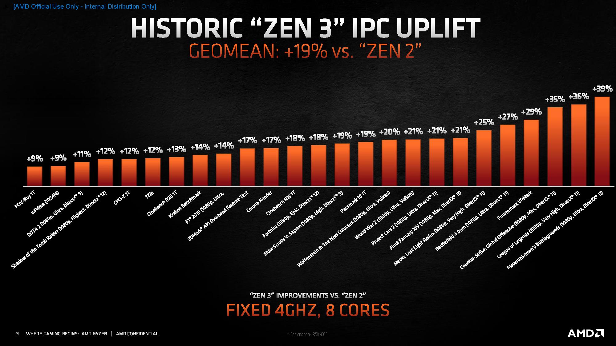
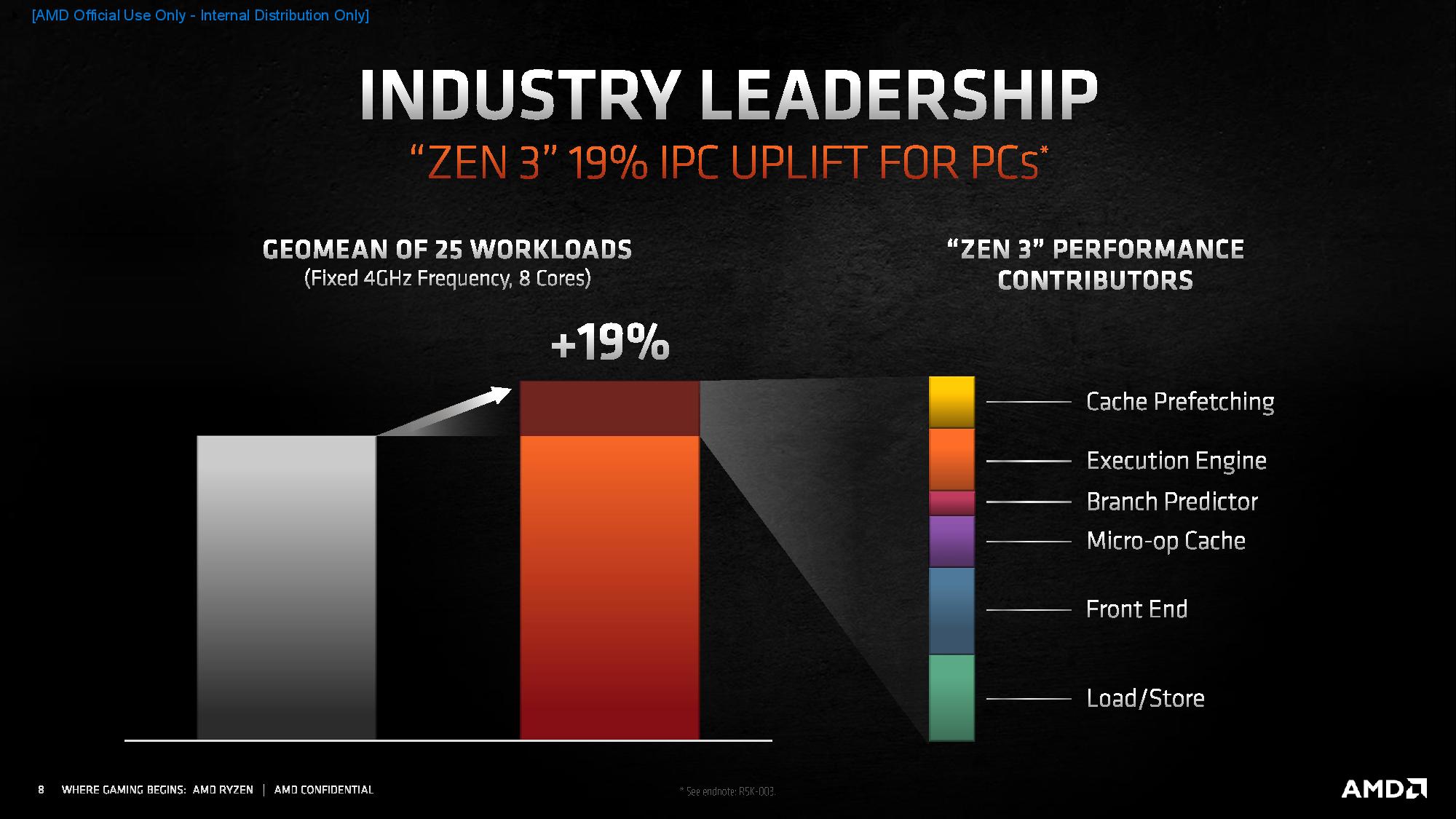
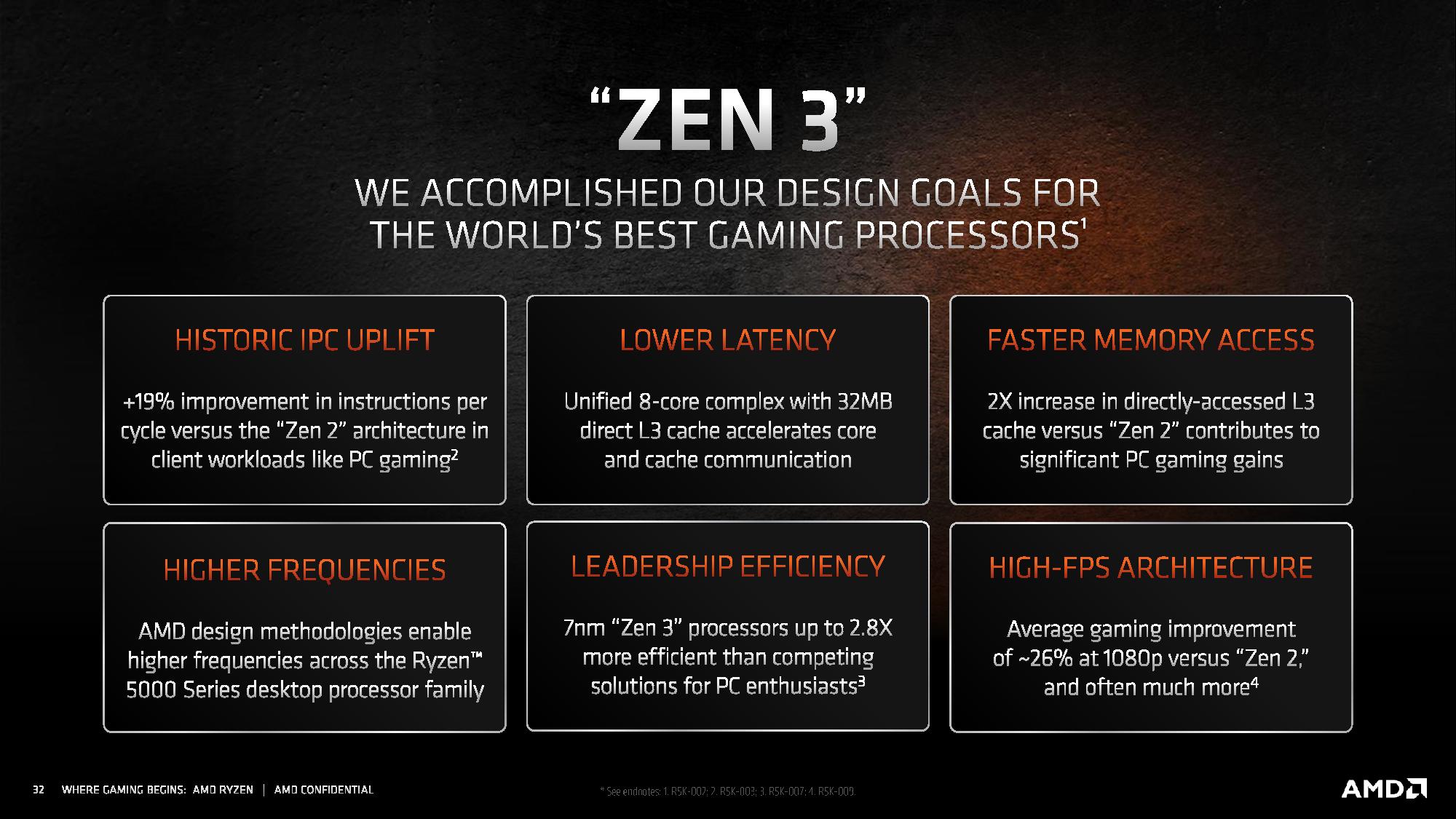
AMD chalks its 19% IPC improvement, which is the largest the company has seen in the post-Zen era, up to a number of Zen 3's architectural improvements. The company calculated its IPC improvements from 25 different workloads, including gaming, which seems a curious addition due to possible graphics-imposed bottlenecks, and some multi-threaded workloads. AMD's results show that the IPC improvements vary based on workloads, with up to a 39% improvement on the high end of the spectrum and a 9% improvement on the lower end.
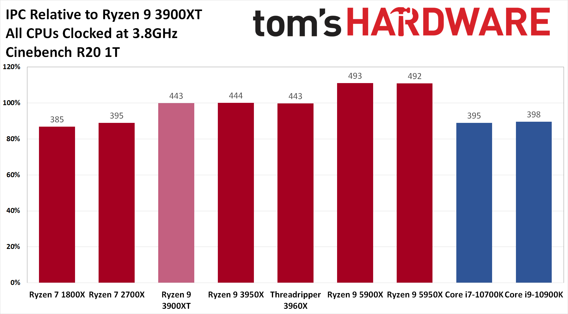
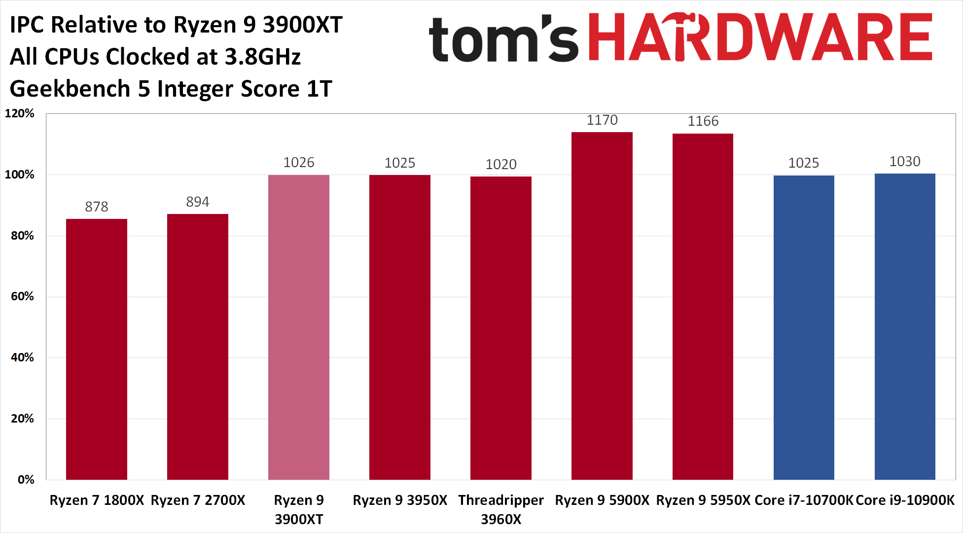
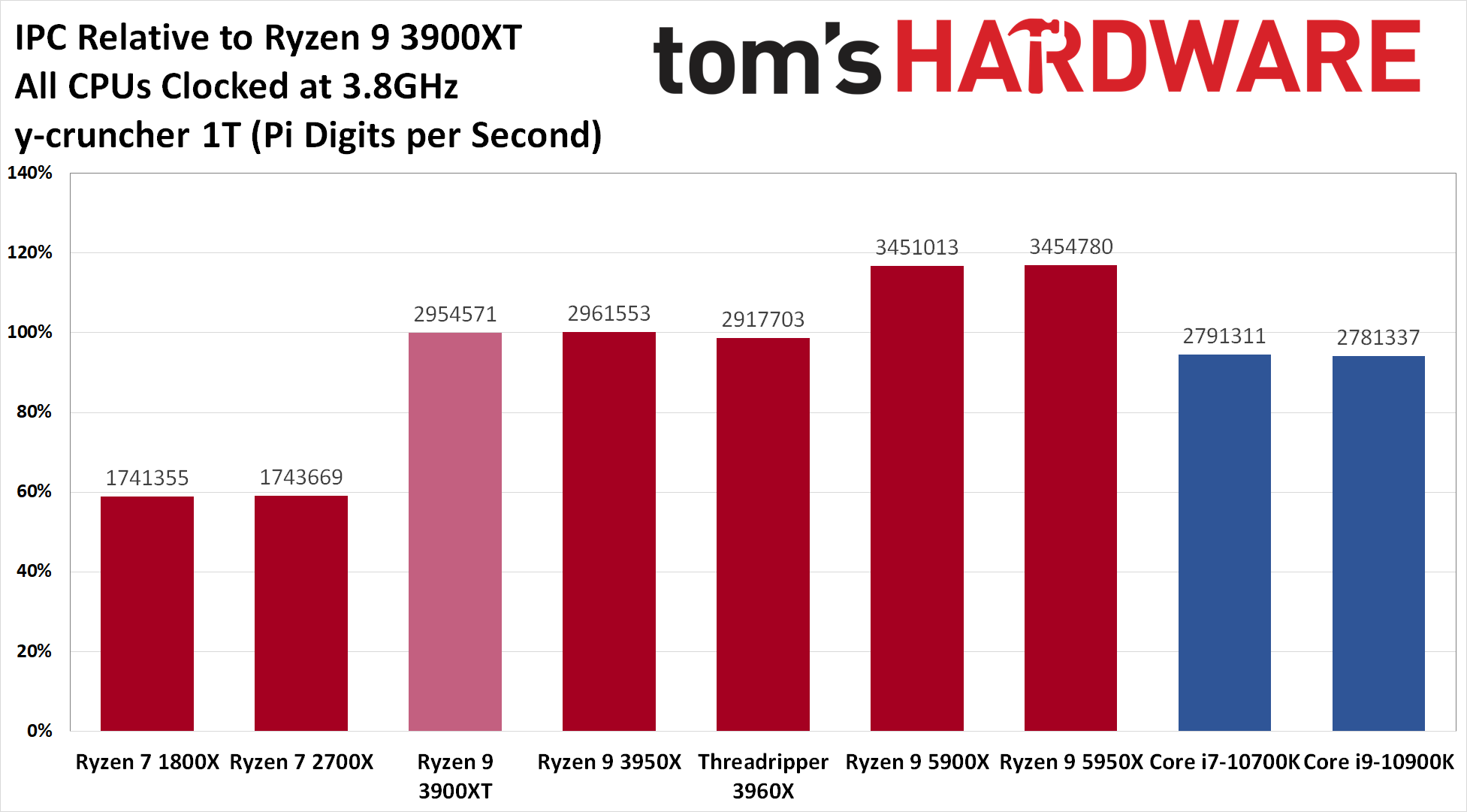
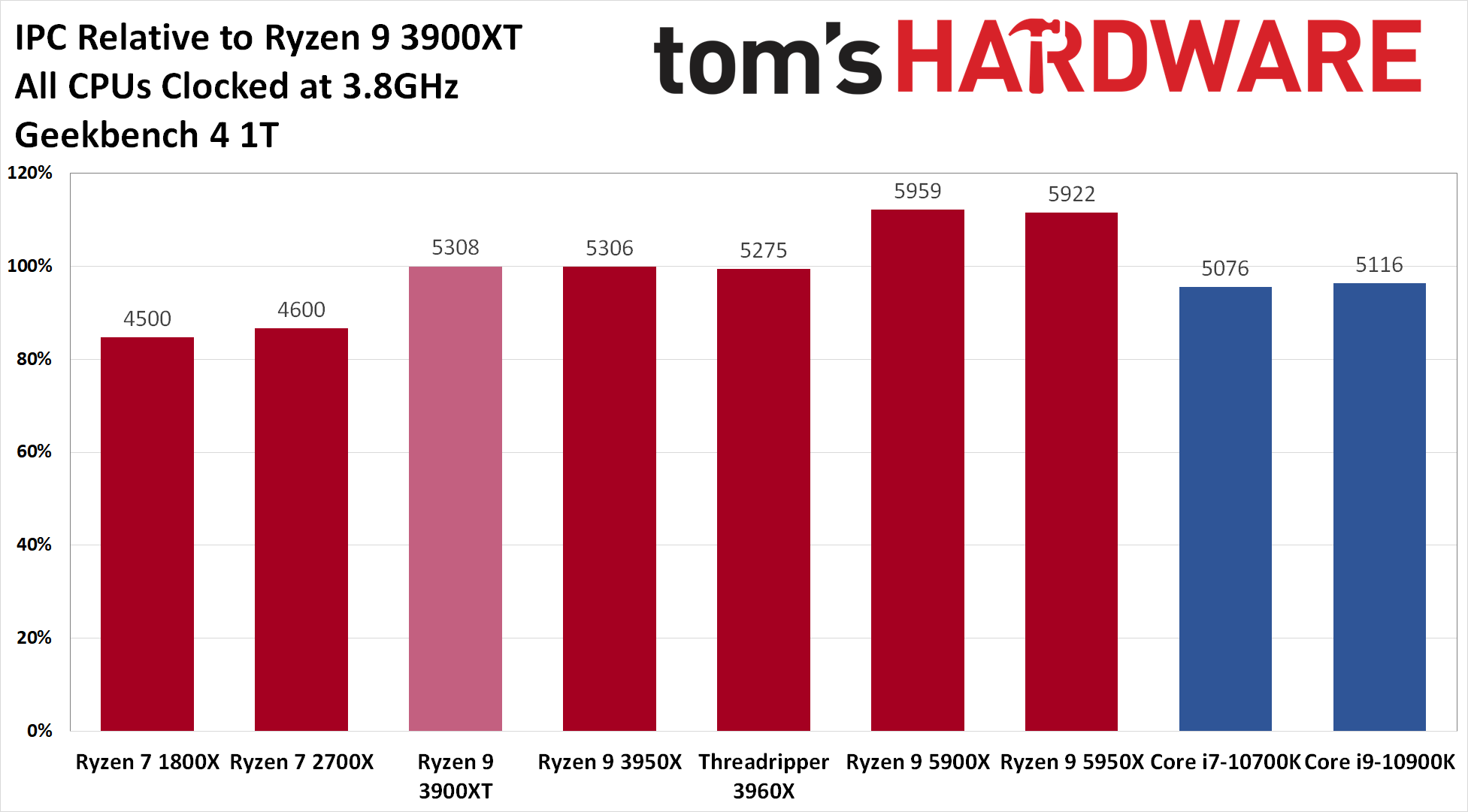
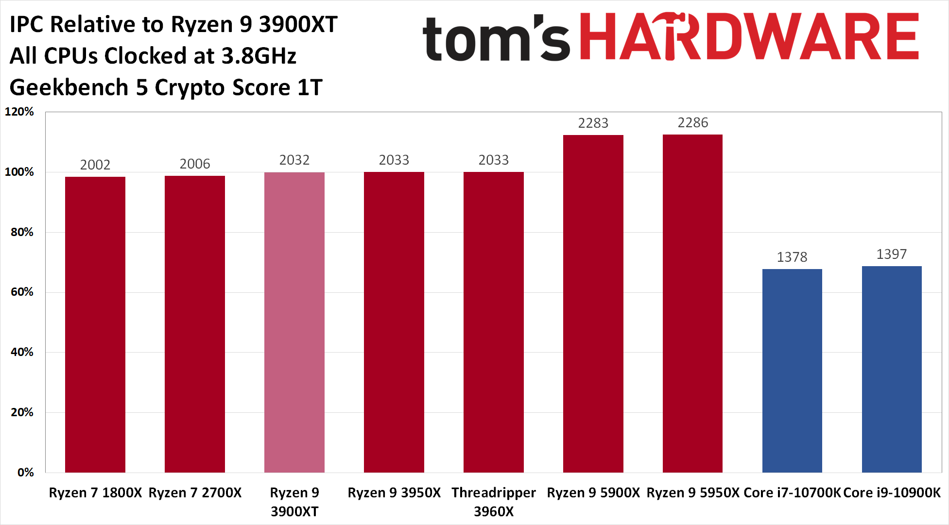
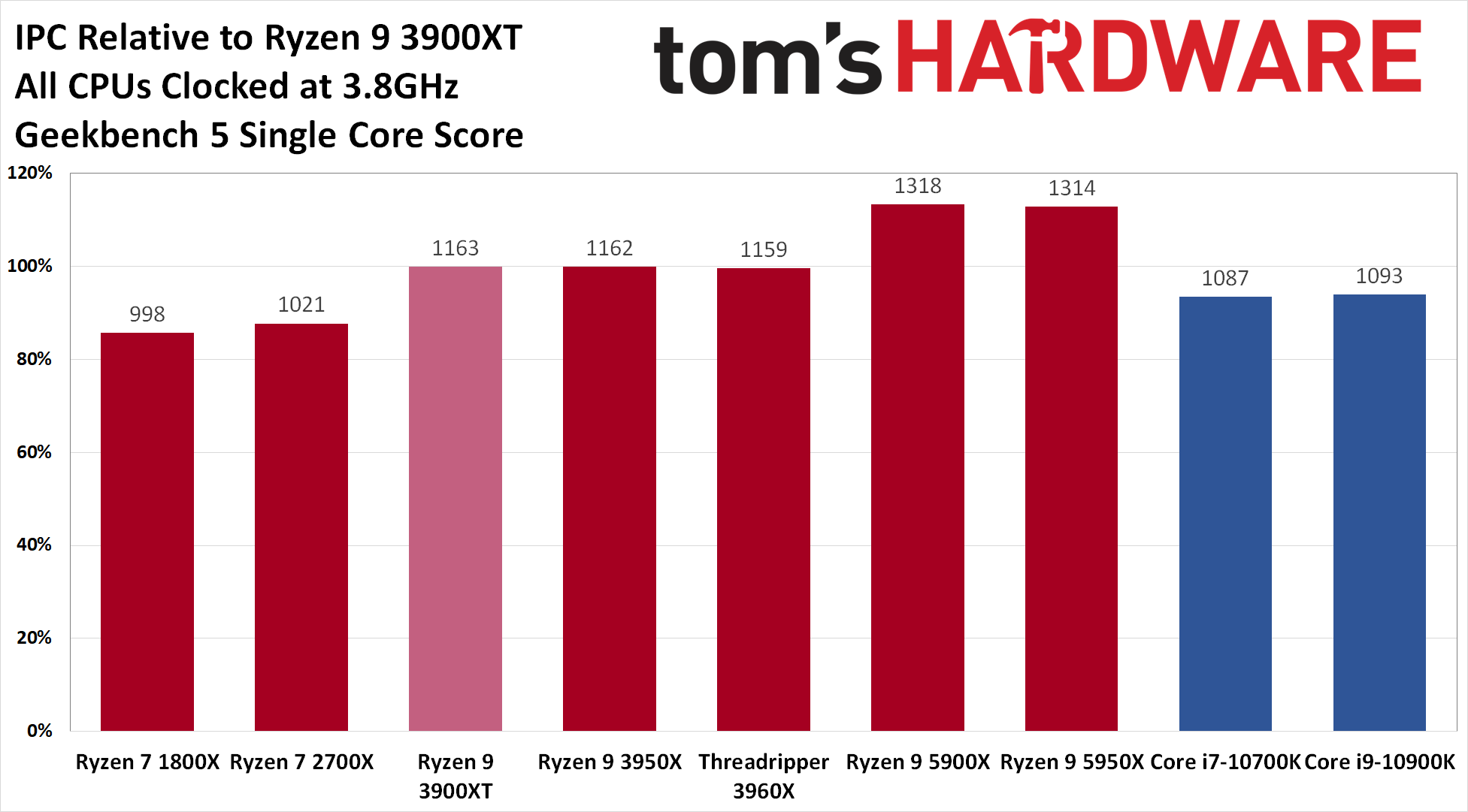
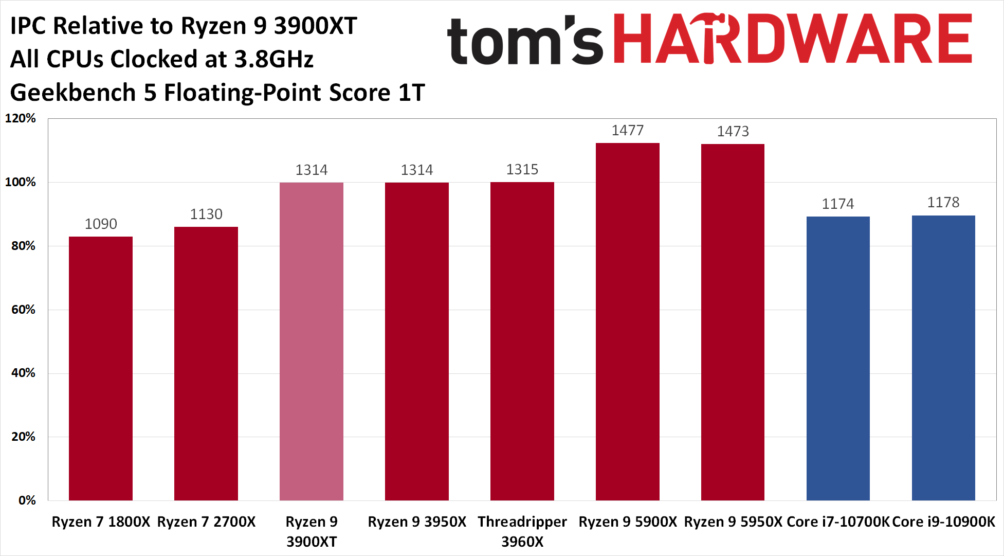
We tested a limited subset of single-threaded workloads to see the clock-for-clock improvements, locking all chips to a static 3.8 GHz all-core clock with the memory dialed into the officially supported transfer rate (AMD used DDR4-3600 for its tests, which is technically an overclocked configuration).
AMD's generational march forward is clear as we move from the left to the right of each chart. Overall, AMD's gen-on-gen IPC increases are exceptional, and Zen 3's IPC obviously beats Intel's Comet Lake chips with ease.
MORE: Best CPUs
MORE: Intel and AMD Processor Benchmark Hierarchy Comparisons
MORE: All CPUs Content
Current page: AMD Zen 3 IPC and Microarchitecture
Prev Page AMD's Magnum Opus Next Page AMD Ryzen 9 5950X and Ryzen 9 5900X Boost Frequency, Overclocking, Test Setup
Paul Alcorn is the Editor-in-Chief for Tom's Hardware US. He also writes news and reviews on CPUs, storage, and enterprise hardware.
-
everettfsargent https://forums.tomshardware.com/threads/amd-ryzen-9-5950x-and-5900x-review-zen-3-breaks-the-5-ghz-barrier.3659689/Reply
Reposting a three week old review? -
everettfsargent Oh and Core i9-10980XE $815 (retail) "You can find the 18-core 36-thread Core i9-10980XE for $815 at several retailers ... " is still a bald-faced lie three weeks later! :(Reply -
VTXcnME Humorous the 'cons' that list price increases of $50. For the last decade, Intels flagship processor has been half again as much as the current Ryzen5000 and so few tech sites batted an eye about it. And it's been a bit since I shopped intel chips, but last I checked, Intel hasn't been bundling coolers with their chips for a while? Someone who follows intel might be able to provide me some guidance there.Reply
As a home building enthusiast (for the last decade or so) this is a very exciting time having legit competition between team red and team blue. Even AMD and Nvidia is getting interesting! A fantastic time to be a home builder. I can't wait to see how intel counter punches here. Should be an interesting decade ahead. -
veldrane2 mmmmkay ........Reply
But can it break the "be actually in stock" barrier ?
Which benchmark tools give us those results ?
I mean ... It does look cute somewhere in the fluffy land of benchmarks and future upcoming products even though "technically" its not a future product. -
JordonB Reply
AMD 5950 selling at $695 on Amazon. It was there last night for sale 1 per person. I was happily surprised. I would have purchased it but had purchased a 3900X 4 months ago.veldrane2 said:mmmmkay ........
But can it break the "be actually in stock" barrier ?
Which benchmark tools give us those results ?
I mean ... It does look cute somewhere in the fluffy land of benchmarks and future upcoming products even though "technically" its not a future product. -
VTXcnME ReplyJordonB said:AMD 5950 selling at $695 on Amazon. It was there last night for sale 1 per person. I was happily surprised. I would have purchased it but had purchased a 3900X 4 months ago.
aaannnnd it's gone again. LOL -
Co BIY These will sell at the premium prices they are asking for. I don't see why they shouldn't. Past AMD chips sold below msrp because they had to be "value" chips but these are performance leaders.Reply
They also probably have limited ability to greatly increase production since TSMC is booked up so they aren't going to increase the volume sold by lowering prices. -
Trustdesa ReplyVTXcnME said:Humorous the 'cons' that list price increases of $50. For the last decade, Intels flagship processor has been half again as much as the current Ryzen5000 and so few tech sites batted an eye about it. And it's been a bit since I shopped intel chips, but last I checked, Intel hasn't been bundling coolers with their chips for a while? Someone who follows intel might be able to provide me some guidance there.
As a home building enthusiast (for the last decade or so) this is a very exciting time having legit competition between team red and team blue. Even AMD and Nvidia is getting interesting! A fantastic time to be a home builder. I can't wait to see how intel counter punches here. Should be an interesting decade ahead.
It also humorous how fanboys cried at Intel "robbing" "price gauging" but now that their master AMD is showing to be as anti consumer, even more so with GPU fanboys defend what they were crying about before. They are both corporates, sorry I hope it won't come as a shook to you :)
It must be sad being a fanboys of a brand making silicon chip...like really sad. Consumer excited by their masters charging more, imagine if Intel or Nvidia or ATI, or S3 or any tech company charged £50 more each generation, a CPU or GPU or Monitor would cost you ehmmm £50k circa if we start from 8086 onwards... I mean guys if you have no economics basis and your jobs do not involve finance perhaps you should not comment :) -
VTXcnME ReplyTrustdesa said:It also humorous how fanboys cried at Intel "robbing" "price gauging" but now that their master AMD is showing to be as anti consumer, even more so with GPU fanboys defend what they were crying about before. They are both corporates, sorry I hope it won't come as a shook to you :)
It must be sad being a fanboys of a brand making silicon chip...like really sad. Consumer excited by their masters charging more, imagine if Intel or Nvidia or ATI, or S3 or any tech company charged £50 more each generation, a CPU or GPU or Monitor would cost you ehmmm £50k circa if we start from 8086 onwards... I mean guys if you have no economics basis and your jobs do not involve finance perhaps you should not comment :)
Remember the time Intel's flagship chip was like $1,400/USD? And intel fanboys cried and fawned in the glory of it's brilliance.
Now AMD has a chip that's more powerful that that, that's still listed for about half of what that intel chip was and it's "price gouging" :ROFLMAO::ROFLMAO::ROFLMAO:
Fanboys of any brand are obnoxious. As an end point consumer, I'm just happy to see actual legit competition between the major CPU and GPU communities. -
drivinfast247 Reply
Not sure if joking or.........Trustdesa said:It also humorous how fanboys cried at Intel "robbing" "price gauging" but now that their master AMD is showing to be as anti consumer, even more so with GPU fanboys defend what they were crying about before. They are both corporates, sorry I hope it won't come as a shook to you :)
It must be sad being a fanboys of a brand making silicon chip...like really sad. Consumer excited by their masters charging more, imagine if Intel or Nvidia or ATI, or S3 or any tech company charged £50 more each generation, a CPU or GPU or Monitor would cost you ehmmm £50k circa if we start from 8086 onwards... I mean guys if you have no economics basis and your jobs do not involve finance perhaps you should not comment :)
