GeForce GTX 680 2 GB Review: Kepler Sends Tahiti On Vacation
Enthusiasts want to know about Nvidia's next-generation architecture so badly that they broke into our content management system and took the data to be used for today's launch. Now we can really answer how Kepler fares against AMD's GCN architecture.
GK104: The Chip And Architecture
GeForce GTX 680’s Vital Signs
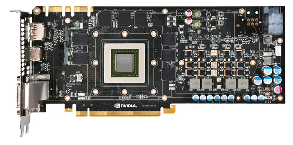
Once we strip the card of its cooling hardware, we’re left with a bare board.
The GK104 GPU sits at its center, composed of 3.54 billion transistors on a 294 mm² die. Again, Nvidia lands between two of AMD’s current-gen offerings: the Tahiti GPU contains 4.31 billion transistors in a 365 mm² die, while Pitcairn is composed of 2.8 billion transistors in a 212 mm² die.
Article continues belowKnowing that GK104 is manufactured on TSMC’s 28 nm node, the GPU’s supply will almost certainly be tight as multiple customers vie for the foundry’s limited output. With that said, the company tells us to expect some availability at launch, with another wave of boards to arrive in early April.
Now, let’s have a look at the GPU’s specifications compared to GeForce GTX 580 and AMD’s Radeon HD 7970:
| Header Cell - Column 0 | GeForce GTX 680 | Radeon HD 7950 | Radeon HD 7970 | GeForce GTX 580 |
|---|---|---|---|---|
| Shaders | 1536 | 1792 | 2048 | 512 |
| Texture Units | 128 | 112 | 128 | 64 |
| Full Color ROPs | 32 | 32 | 32 | 48 |
| Graphics Clock | 1006 MHz | 800 MHz | 925 MHz | 772 MHz |
| Texture Fillrate | 128.8 Gtex/s | 89.6 Gtex/s | 118.4 Gtex/s | 49.4 Gtex/s |
| Memory Clock | 1502 MHz | 1250 MHz | 1375 MHz | 1002 MHz |
| Memory Bus | 256-bit | 384-bit | 384-bit | 384-bit |
| Memory Bandwidth | 192.3 GB/s | 240 GB/s | 264 GB/s | 192.4 GB/s |
| Graphics RAM | 2 GB GDDR5 | 3 GB GDDR5 | 3 GB GDDR5 | 1.5 GB GDDR5 |
| Die Size | 294 mm2 | 365 mm2 | 365 mm2 | 520 mm2 |
| Transistors (Billion) | 3.54 | 4.31 | 4.31 | 3 |
| Process Technology | 28 nm | 28 nm | 28 nm | 40 nm |
| Power Connectors | 2 x 6-pin | 2 x 6-pin | 1 x 8-pin, 1 x 6-pin | 1 x 8-pin, 1 x 6-pin |
| Maximum Power | 195 W | 200 W | 250 W | 244 W |
| Price (Street) | $510 | $450 | $550 | ~$410 |
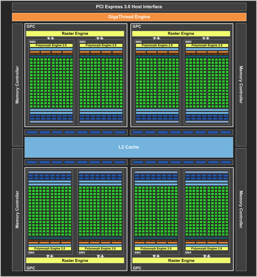
The GK104 GPU is broken down into four Graphics Processing Clusters (GPCs), each of which contains two Streaming Multiprocessors (formerly referred to as SMs, and now called SMXs).
While there’s undoubtedly a lot of depth we could go into on the evolution from the original GF100 design to the GK104 architecture debuting today, the easiest way to characterize this new chip is in reference to the GF104 processor that first powered GeForce GTX 460.
Get Tom's Hardware's best news and in-depth reviews, straight to your inbox.
In comparison to GF104's SM, the GK104 SMXs features two times as many warp schedulers (from two up to four), dispatch units (from four up to eight), and texture units (from eight up to 16) per Shader Multiprocessor, along with a register file that’s twice as large. It also sports four times as many CUDA cores. GF104 included 48 shaders per SM; GK104 ups that to 192 shaders in each SMX.
| GK104 SMX (Left) Versus GF104 SM (Right) |
Per SM:GK104GF104RatioCUDA Cores192484xSpecial Function Units3284xLoad/Store32162xTexture Units1682xWarp Schedulers422xGeometry Engines111x
Why quadruple the number of CUDA cores and double the other resources? Kepler’s shaders run at the processor’s frequency (1:1). Previous-generation architectures (everything since G80, that is) operated the shaders two times faster than the core (2:1). Thus, doubling shader throughput at a given clock rate requires four times as many cores running at half-speed.
The question then becomes: Why on earth would Nvidia throttle back its shader clock in the first place? It’s all about the delicate balance of performance, power, and die space, baby. Fermi allowed Nvidia’s architects to optimize for area. Fewer cores take up less space, after all. But running them twice as fast required much higher clock power. Kepler, on the other hand, is tuned for efficiency. Halving the shader clock slashes power consumption. However, comparable performance necessitates two times as many data paths. The result is that Kepler trades off die size for some reduction in power on the logic side, and more significant savings from clocking.
Additional die area and power are cut by eliminating some of the multi-ported hardware structures used to help schedule warps and moving that work to software. By minimizing the amount of power and area consumed by control logic, more space is freed up for doing useful work versus Fermi.
Nvidia claims that the underlying changes made to its SMX architecture result in a theoretical doubling of performance per watt compared to Kepler’s predecessor—and this is actually something we’ll be testing today.
Alright. We have eight of these SMXs, each with 192 CUDA cores, adding up to 1536. Sixteen texture units per SMX yield 128 in a fully-enabled GK104 processor. And one geometry engine per SMX gives us a total of eight. Now, wait a minute—GF104 had eight PolyMorph engines, too. So Nvidia multiplied all of these other resources out, but left its primitive performance alone? Not quite.
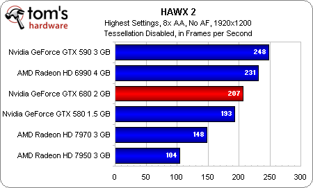
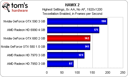
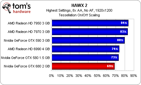
To begin, Nvidia claims that each PolyMorph engine is redesigned to deliver close to two times the per-clock performance of Fermi’s fixed-function geometry logic. This improvement is primarily observable in synthetic metrics, which we’ve seen developers (rightly) argue should represent the future of their efforts, exploiting significantly more geometry than today’s titles to augment realism. But if you’re playing something available right now, like HAWX 2, how can you expect Kepler to behave?
In absolute terms, GeForce GTX 680 easily outperforms the Radeon HD 7970 and 7950, regardless of whether tessellation is used or not. However, Nvidia’s new card takes a 31% performance hit when you toggle tessellation on in the game’s settings. In comparison, the Tahiti-based Radeons take a roughly 16% ding. Now, there’s a lot more going on in a game than just tessellation to affect overall performance. But it’s still interesting to note that, in today’s titles, the advantage Nvidia claims doesn’t necessarily pan out.
In order to support the theoretically-higher throughput of its geometry block, Nvidia also doubles the number of raster engines compared to GF104, striking a 1:1 ratio with the ROP partitions.
Like GF104, each of GK104’s ROPs outputs eight 32-bit integer pixels per clock, adding up to 32. The two GPUs also share 256-bit aggregate memory buses in common. Where they differ is maximum memory bandwidth.
Perhaps more true to its mid-range price point, GeForce GTX 460 included up to 1 GB of GDDR5 running at 900 MHz, yielding 115.2 GB/s. GeForce GTX 680 is being groomed to succeed GeForce GTX 580, though, which utilized 1002 MHz GDDR5 on a 384-bit aggregate bus to serve up 192.4 GB/s of throughput. Thus, GeForce GTX 680 comes armed with 2 GB of GDDR5 operating at 1502 MHz, resulting in a very similar 192.26 GB/s figure.
Current page: GK104: The Chip And Architecture
Prev Page GeForce GTX 680: The Card And Cooling Next Page GPU Boost: Graphics Afterburners-
outlw6669 Nice results, this is how the transition to 28nm should be.Reply
Now we just need prices to start dropping, although significant drops will probably not come until the GK110 is released :/ -
Scotty99 Its a midrange card, anyone who disagrees is plain wrong. Thats not to say its a bad card, what happened here is nvidia is so far ahead of AMD in tech that the mid range card purposed to fill the 560ti in the lineup actually competed with AMD's flagship. If you dont believe me that is fine, you will see in a couple months when the actual flagship comes out, the ones with the 384 bit interface.Reply -
Chainzsaw Wow not too bad. Looks like the 680 is actually cheaper than the 7970 right now, about 50$, and generally beats the 7970, but obviously not at everything.Reply
Good going Nvidia... -
rantoc 2x of thoose ordered and will be delivered tomorrow, will be a nice geeky weekend for sure =)Reply
