GeForce GTX 295 Vs. GTX 275 SLI: When Two Are Better Than One

Introduction
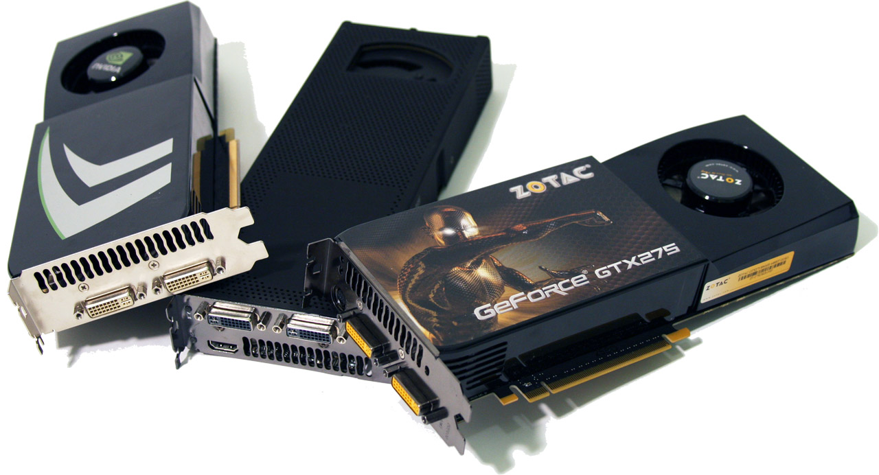
The GeForce GTX 275, launched last month, gives us an opportunity to run some interesting thought experiments using Nvidia’s SLI multi-GPU rendering technology.
You see, the graphics processor driving the GTX 275—a 55nm mash-up somewhere between the GeForce GTX 280 and 260—sports the same configuration found in the company’s GeForce GTX 295 (doubled, of course). By putting a pair of GTX 275s up against a GTX 295, we’re essentially able to test one graphics solution operating over the throughput of a single 16-lane PCI Express 2.0 slot against the same arrangement running across two x16 slots.
With all of the core, shader, and memory clocks set to the same frequencies, the only real variable here would seem to be the amount of PCI Express bandwidth available to your SLI setup. In both situations, separate PCBs are attached with Nvidia’s SLI connector. But the story isn’t quite that simple and, as we’ll see in the benchmarks, the performance results don’t always reflect an advantage in one direction or the other.
There’s another little twist that lets us add a third set of numbers to our comparison here. Mainly, GeForce GTX 275s run at faster speeds than the core/shader/memory used on the GTX 295. So, in order to make a straight comparison, we actually have to down-clock our reference cards to sync up with Nvidia’s fastest offering. Allowed to operate at their default speeds, though, we’d expect the GeForce GTX 275s to be faster.
That’s great news for the gamers who were originally eying a single GeForce GTX 295 and not necessarily planning to spend another $500+ on a second board for quad-SLI. It’s even better when you start taking a look at the current state of GeForce GTX 295 availability (read: sparse). As of this writing, there’s only one card available from Newegg—EVGA’s $589 Red Edition board, which has been marked up exorbitantly for its Ferrari red shroud. A pair of GeForce GTX 275s, on the other hand, go for about $239 each.
So what’s the gamer with a little spare dosh in his pocket to do? Let’s dig a little farther into what makes a GeForce GTX 295 more than just two GTX 275s pasted together, along with some of the other variables you’d want to consider—like power, heat, and room on your motherboard.
The Anatomy Of A GTX 295
Get Tom's Hardware's best news and in-depth reviews, straight to your inbox.
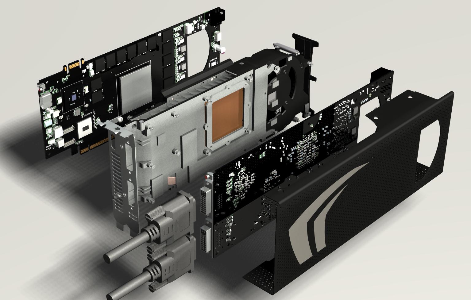
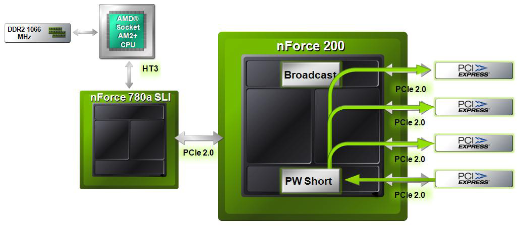
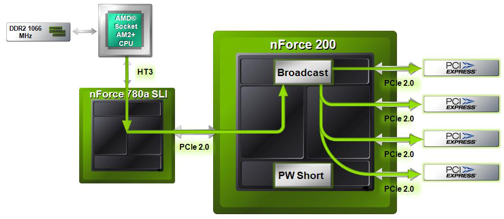
At its most fundamental level, the GeForce GTX 295 really is two GeForce GTX 275-class boards sandwiched together in a dual-slot package. The pair is connected in three different regards: the SLI connector that’d normally snake over the top of two separate boards, S/PDIF pass-through (to let one signal be used by both PCBs), and PCI Express data going to/from the BR04 (known as nForce 200) bridge chip that resides onboard. Each PCB gets power from a seperate auxiliary plug.
According to Nvidia’s SLI Zone page, “the SLI connector is a proprietary link between GPUs that transmits synchronization, display, and pixel data. The SLI connector enables inter-GPU communication of up to 1GB/s, consuming no bandwidth over the PCI Express bus.” Now, the current implementation of the SLI connector actually moves more than 1 GB/s of information, but Nvidia won’t say exactly fast that interconnect is clocked for this generation of cards.
Moreover, it’s hard to say (without seeing the benchmark results): first, how much the latencies of adding that BR04 bridge might hurt performance or, second, how much the benefits of adding PWShort (Nvidia’s GPU-to-GPU link) and broadcast capabilities might improve performance. We’re sure gunning to find out, though.
-
imrul "Intel Core i7 920 Extreme (Bloomfield)" (page 3)Reply
there's no extreme version of i7 920, nor is it bloomfield... -
reasonablevoice What the hell is up with the underclocked cards out performing the others in that H.A.W.X.Reply
Can the author of the article comment with what they think is going on there? -
cangelini reasonablevoiceWhat the hell is up with the underclocked cards out performing the others in that H.A.W.X.Can the author of the article comment with what they think is going on there?Reply
Happened in WiC w/o AA as well. Difficult to say went on there, but the results are repeatable. Probably more important, though, is that when more of an emphasis is put on the graphics subsystem, you see those stock-clocked boards take the lead, as we'd expect. -
avatar_raq 1.Very good article, unlike some other author's articles in this site, this article is solid (starting from the test system down to the conclusion) and interesting, this is what I always expect from Chris.Reply
2.As for the strange issue in L4D, HAWX and WIC where the slower 275s beat the faster ones....Odd indeed. Is there any chance the normally clocked cards automatically clocked down to 2D mode or somthing in-game? In other words the GPUs usage dropped due to the CPU bottleneck or whatever, and the cards' driver decided to clockdown to save energy! I've seen nvidia and ati cards do that. The monitoring utility of rivatuner could have revealed such things since it shows real-time clocks..BTW what software did you use to downclock?
It would be funny to consider downclocking our cards to 'gain' performance!!
3.I hope the new (single PCB) 295 will drop in larger quantities, perhaps it will be more practical than the current one, and will tip the balnce here in its favor.
http://www.techpowerup.com/img/09-05-12/13c.jpg -
Can you put the "online shop" section underneath the "Next" button for the next page...its really annoying and inconvenient to have it positioned within the article as it seems to be.Reply
Thanks
-
JeanLuc rags_20Please benchmark in Very High.Reply
I noticed that to, if I owned that kind of hardware I would be playing every game at the highest settings even if it is Crysis.


