GK110: The True Tank
Think back to Nvidia’s last generation of graphics cards, the Fermi-based 500-series. For each of its GPUs, the company’s marketing team came up with different battlefield classes: the tank, the hunter, and the sniper, each configuration optimized for a different role. The GeForce GTX 580’s GF110 was the heavy-hitting tank. Big, powerful, and expensive, it represented the Fermi architecture’s maximum potential.

In comparison, we knew right out of the gate that the GeForce GTX 680’s GPU was no GF110-successor, even though Nvidia wanted $500 for the privilege of owning one. GK104 is optimized for gaming and it sacrificed compute performance in a dramatic way, underperforming the 580 in our OpenCL-based tests. At the time, Nvidia downplayed the significance of GK104’s compromises, preferring to instead hammer home how well its 3.5 billion transistor chip did against AMD’s 4.3 billion transistor Tahiti GPU in games.
But then the company introduced its Tesla K20 family, powered by GK110—the true tank (even if Nvidia isn’t using that parallel any more).
Inside The SMX
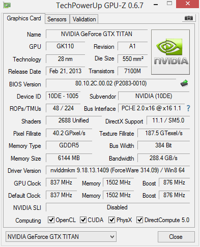
A complete GK110 GPU consists of 15 Streaming Multiprocessors, which, remember, now go by the name SMX. These SMX blocks are largely the same as they are in GK104, powering GeForce GTX 680. They still include 192 CUDA cores, 16 texture units, and very similar cache structures. But there are obviously a lot more of them. GK104 includes eight SMX blocks. GK110 hosts 15. Because the chip is so big and complex, though, defects seriously affect yields. Perfectly-manufactured GPUs undoubtedly exist. However, even the highest-end GK110-based products have one disabled SMX. Multiply out 192 shaders 14 times, and you get a GPU with 2,688 CUDA cores. Moreover, 16 texture units for each of 14 SMXes gives you a total of 224 TMUs, up from GeForce GTX 680’s 128.
| Per SMX: | GF100 (Fermi) | GF104 (Fermi) | GK110 (Kepler) | GK104 (Kepler) |
|---|---|---|---|---|
| CUDA Compute Capability | 2.0 | 2.0 | 3.5 | 3.0 |
| Threads/Warp | 32 | 32 | 32 | 32 |
| Maximum Warps/SMX | 48 | 48 | 64 | 64 |
| Maximum Threads/SMX | 1,536 | 1,536 | 2,048 | 2,048 |
| Maximum Thread Blocks/SMX | 8 | 8 | 16 | 16 |
| 32-bit Registers/SMX | 32,768 | 32,768 | 65,536 | 65,536 |
| Maximum Registers/Thread | 63 | 63 | 255 | 63 |
| Maximum Threads/Thread Block | 1,024 | 1,024 | 1,024 | 1,024 |
Beyond simply piling on additional resources that accelerate gaming, GK110 addresses the “hunter’s” most glaring shortcoming (particularly if you consider GeForce GTX 680 a replacement for GeForce GTX 580): its compute potential. In GK104, each SMX features 192 FP32-capable cores, yielding more than 3 TFLOPS of peak floating-point performance. But you only get eight FP64 units, capping double-precision performance to 1/24 of the FP32 rate. A GK110 SMX incorporates 64 FP64 CUDA cores, narrowing that ratio to 1/3. Nvidia says a GeForce GTX Titan offers up to 4.5 TFLOPS of single-precision and 1.5 TFLOPS of peak double-precision compute power. In theory, that puts it just ahead of AMD’s Radeon HD 7970 GHz Edition card, rated for 4.3 TFLOPS of single- and 1.01 TFLOPS of double-precision performance.


We’re naturally happy to see GK110 bring an emphasis back onto compute. However, there’s no question that GeForce GTX Titan’s ability to cut through real-time graphics is top priority. In order to balance that 75% increase in shader and texture unit count, Nvidia also bolsters the GPU’s back-end. GK104’s four ROP partitions are able to output eight 32-bit integer pixels per clock, adding up to what the company calls 32 ROP units. GK110 leverages six of those blocks, increasing that number to 48.
Both the GeForce GTX 680 and Titan employ GDDR5 memory running at 1,502 MHz. But because GK110 features six 64-bit memory interfaces, rather than GK104’s four, peak bandwidth increases 50% from 192 GB/s to 288 GB/s. That matches AMD’s reference Radeon HD 7970 GHz Edition card, which also sports 1,500 MHz GDDR5 on a 384-bit bus.
