Nvidia GeForce GTX 1060 Graphics Card Roundup
Nvidia GeForce GTX 1060 Founders Edition
Why you can trust Tom's Hardware
For a reference design - sorry, Founders Edition - this card's appearance is quite neat. But are there any good reasons to pick Nvidia's implementation over competing models? After all, it's heavy and employs a completely different cooling solution than the competition.
Technical Specifications
MORE: Best Graphics Cards
MORE: Desktop GPU Performance Hierarchy Table
MORE: All Graphics Content
Exterior & Interfaces
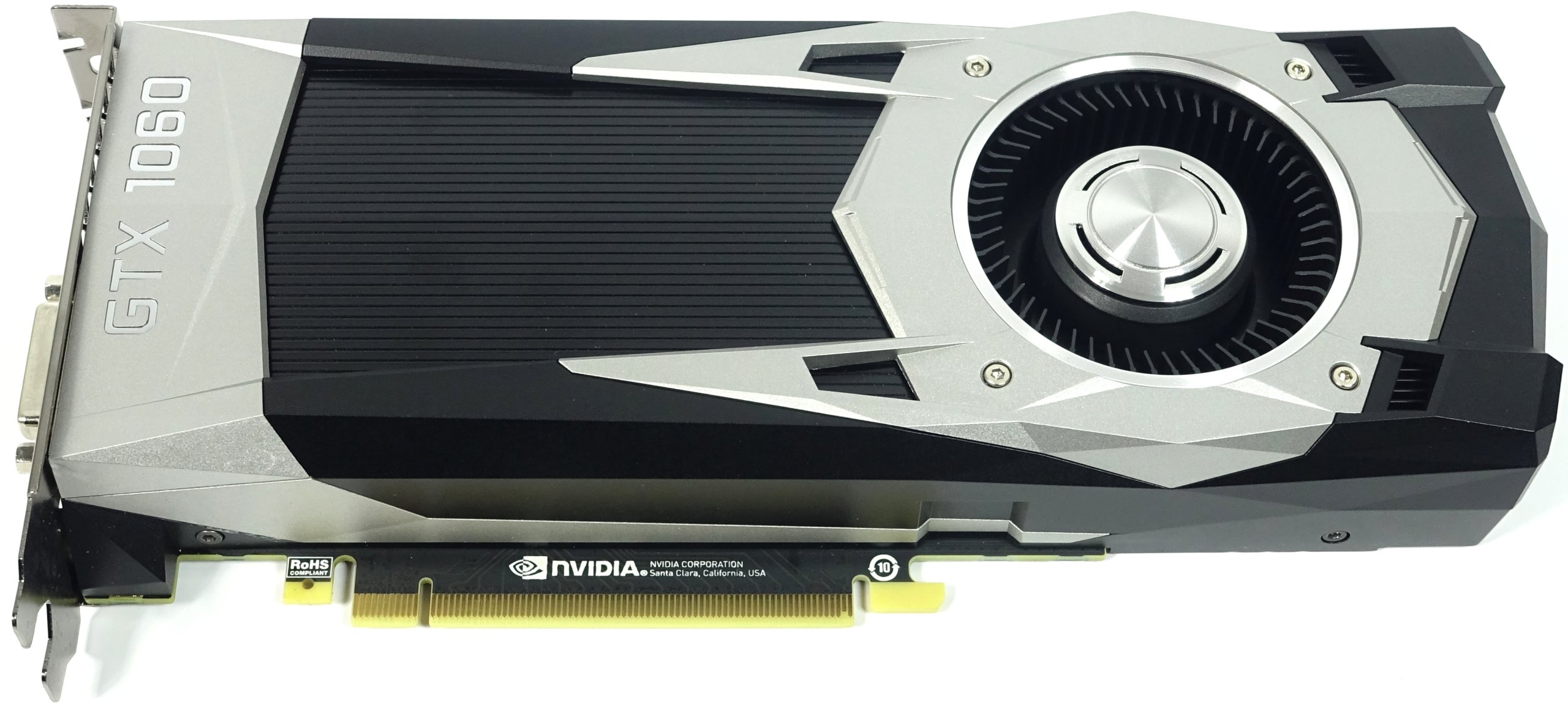
Despite using a much shorter PCB, Nvidia's Founders Edition is still 10 inches (25.4cm) long. It is 4¼ inches (10.7cm) tall and 1½ inches (3.8cm) wide, too. The slot bracket is the widest part. Behind it, the card and cooler only measure about 3.5cm together.
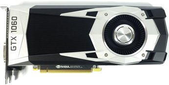
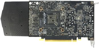
For the shroud, Nvidia again uses a mix of aluminum and plastic. This time the company favors economy, though. The cover can be detached in one piece, including the fan.
There's still an illuminated GeForce GTX logo up top, and the cooler's internals are completely hidden.
In contrast to the coolers you often seen on cards with short PCBs, the housing's overhang doesn't have a hole to feed the fan with air. Instead, the back side is covered. There is no backplate either, further reducing cost.
The back hosts Nvidia's well-known, gill-shaped air intakes. These are more fragile, so you'll want to be careful positioning this card in a case.

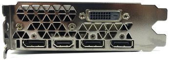
The output bracket carries over from Nvidia's GeForce GTX 1070 and 1080 Founders Editions. It's dominated by three DisplayPort 1.4-ready connectors, one HDMI 2.0 output, and one dual-link DVI-D interface.
Board & Components
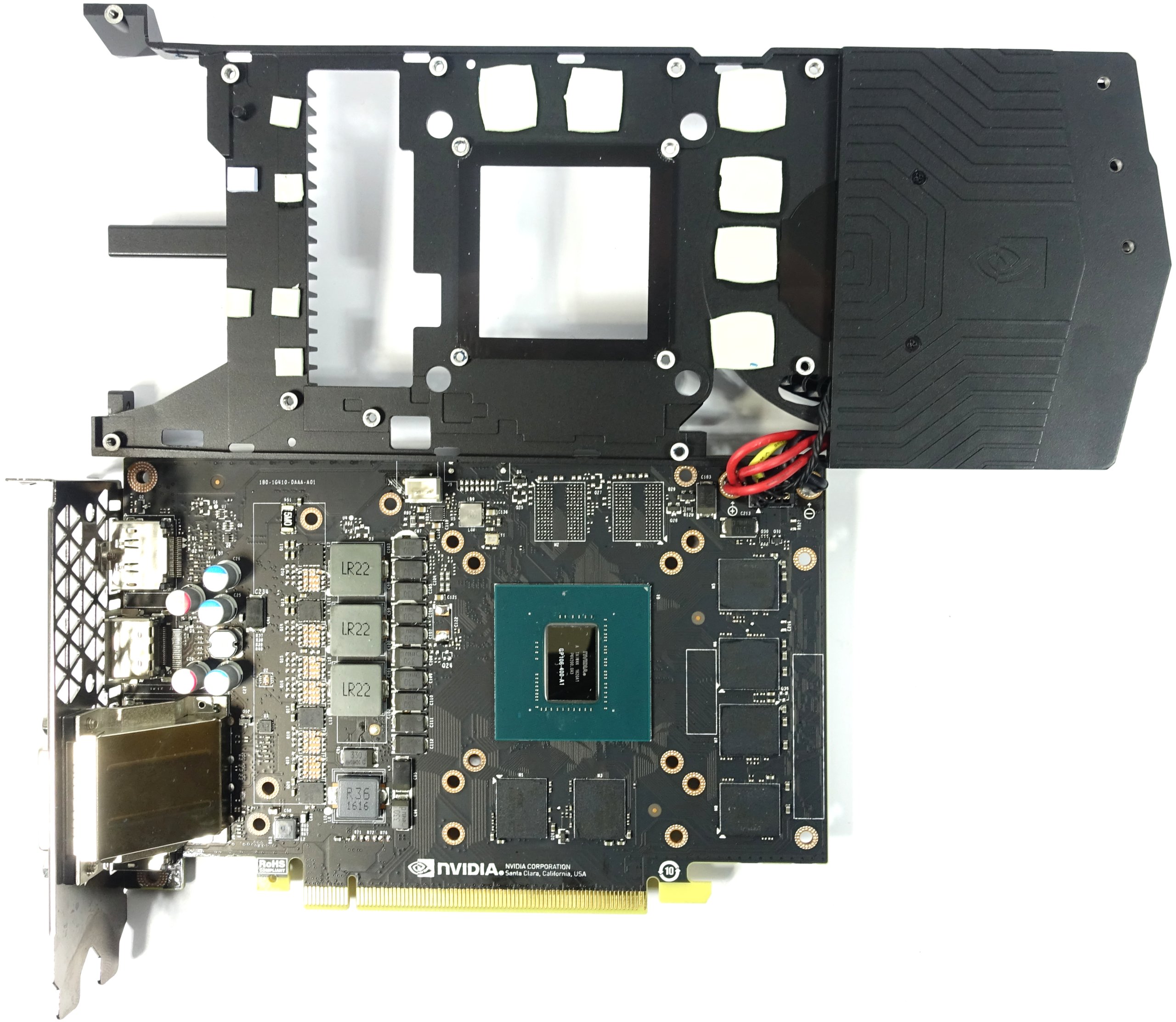
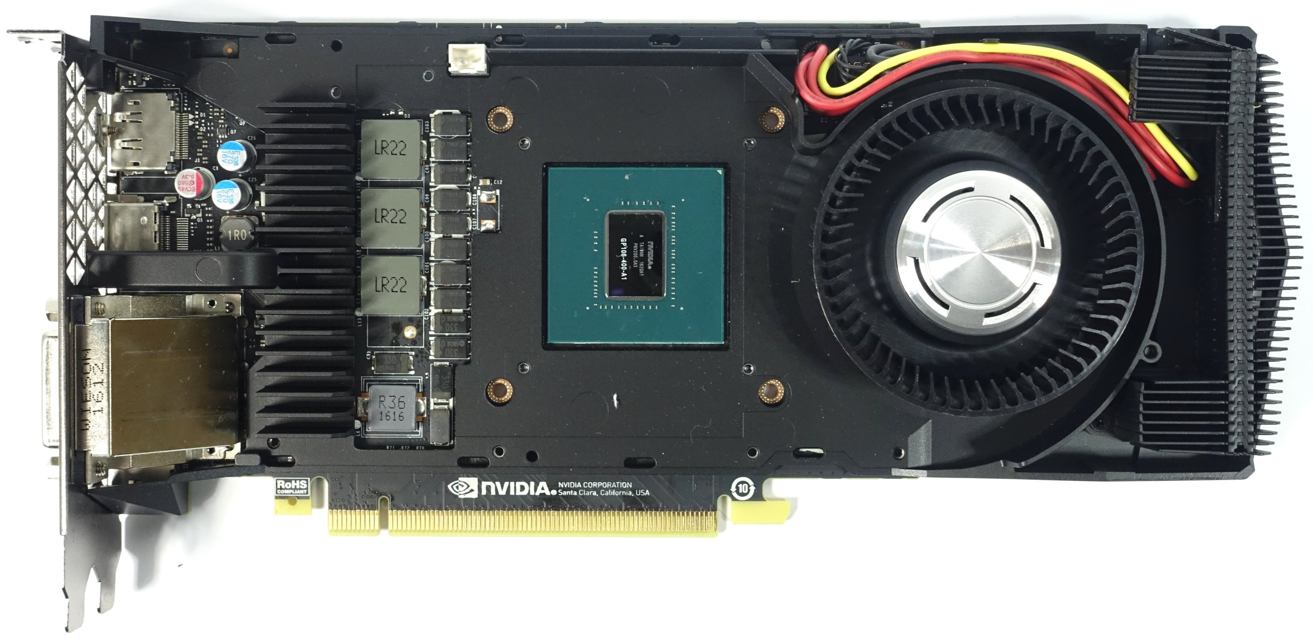
The center of the card is naturally dominated by its graphics processor, even if the GP106-400-A1 is significantly smaller than the GP104 on GeForce GTX 1070 and 1080. There are other noticeable differences as well, like the on-board memory. Nvidia's GeForce GTX 1060 only uses six of the available eight module emplacements, each populated with Samsung K4G80325FB-HC25 ICs. The modules have a capacity of 8Gb (32x 256Mb), and operate between 1.305 and 1.597V, depending on clock rate. In total, they add up to 6GB of GDDR5.
Unfortunately, the PWM controller isn't documented. It’s made by uPI Semiconductor and bears the model number uP9509, which means that it’s probably the uP9511P’s smaller sibling (the latter controller is what we found paired to the GP104 processor).
The memory modules and one of the GPU phases get their power through the motherboard’s PCIe slot. The two remaining GPU phases and the card’s accessories draw power from the six-pin power connector. We'll take a closer look at what this means in terms of load distribution across the rails on the next page.
When it comes to voltage regulation, Nvidia uses only one Dual N-Channel MOSFET, the E6930, per phase for both the high and low side; separate gate drivers aren’t needed. This highly integrated component explains the empty spaces on the board.
The GPU’s three phases are completely sufficient, and their distribution makes more sense here than on AMD's Radeon RX 480.
Apart from the six-pin power connector, which appears to have taken a wrong turn somewhere, Nvidia's reference GeForce GTX 1060 actually looks pretty good. And given a relatively low amount of waste heat, its axial fan isn't a bad choice either.
Power Results
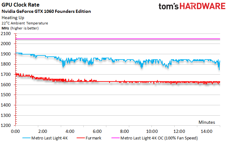
The GeForce GTX 1060 FE does hit its power and temperature limits.
In order to test overclocking, then, we not only increased the GPU Boost frequency, but also the power target to 116 percent while setting the fan to 100 percent. The results certainly speak for themselves, too. Our sample held a stable 2050 MHz through the most taxing passages of our test sequence. Without this forced bit of headroom and the additional fan speed, though, the graphs look shakier:
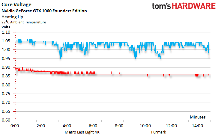
For comparison, let’s take a look at the voltages during normal operation as well. It’s plain to see that the GPU Boost clock and voltages drop once the limit is reached.
The lowest GPU frequency measured at idle was 139 MHz.
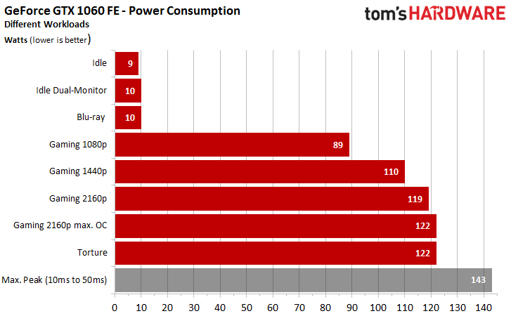
We took our measurements using a variable low-pass filter, so we mention short load peaks only as a side note (see the grayed-out bar in the chart below), since they're rarely relevant in practice.
Power Connector Load
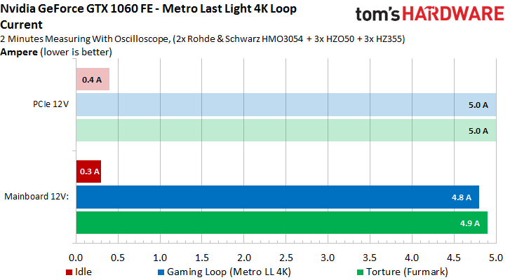
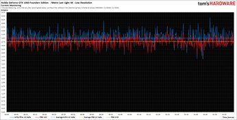
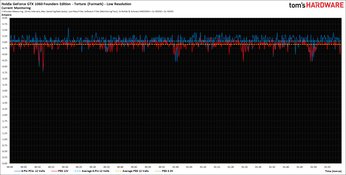
Now we're getting into the nitty gritty. Measurements across the different rails during our taxing gaming and stress tests show that Nvidia manages to distribute the load well with a bias to the six-pin power connector. The 3.3V rail isn't used anymore, which is why you won't find it in our charts.
Here are the detailed graphs. Clicking on them brings up the high-resolution versions.
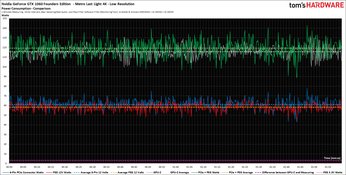
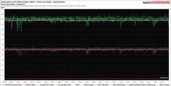
The PCI-SIG’s technical specifications cover current exclusively, so that’s what’s shown in the chart below (power consumption only tells half of the story, after all). With less than 5A for the motherboard slot, Nvidia plays it safe with its GeForce GTX 1060. The maximum, according to the PCI-SIG, is 5.5A.
We have detailed graphs for the current measurements as well. Once again, clicking on them brings up the high-resolution versions.
Temperature Results
Up top, we immediately notice the power connector's strange position. It’s situated in a part of the cooler that protrudes beyond the actual PCA. This necessitates a number of cables to attach to the board.
The implementation is anything but elegant, and it prevents Nvidia's partners from building shorter 1060s. Although the card is only 17.5cm long, it doesn't have any space to accommodate a power connector.

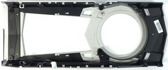
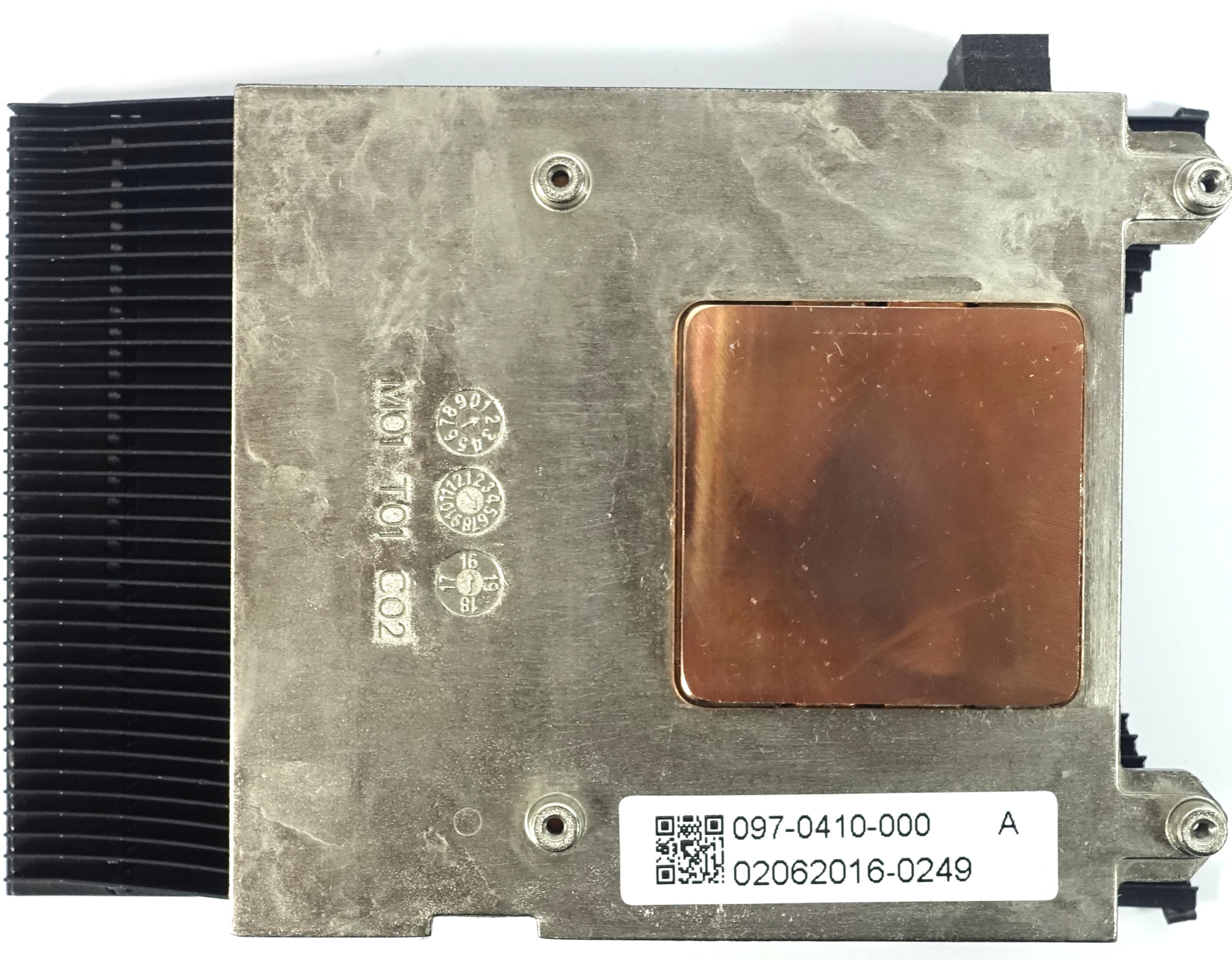
Remove the four screws securing the cooler's body and it comes right off. There’s a massive copper heat sink and metal frame underneath. The closed cooling fin design reminds us of the GeForce GTX 1070, and it should provide ample performance given the 1060's 120W TDP.
The massive frame serves double duty by keeping everything in place and cooling the voltage regulation circuitry/memory modules.
The GeForce GTX 1060 generates similar numbers during the gaming loop (119W) and stress test (122W). In light of this, it’s hardly surprising that the two temperature curves look a lot alike. GPU Boost 3.0 is very restrictive (or already well-optimized, if you prefer). It adjusts the clock rate and voltage to keep the card exactly where it’s supposed to be.
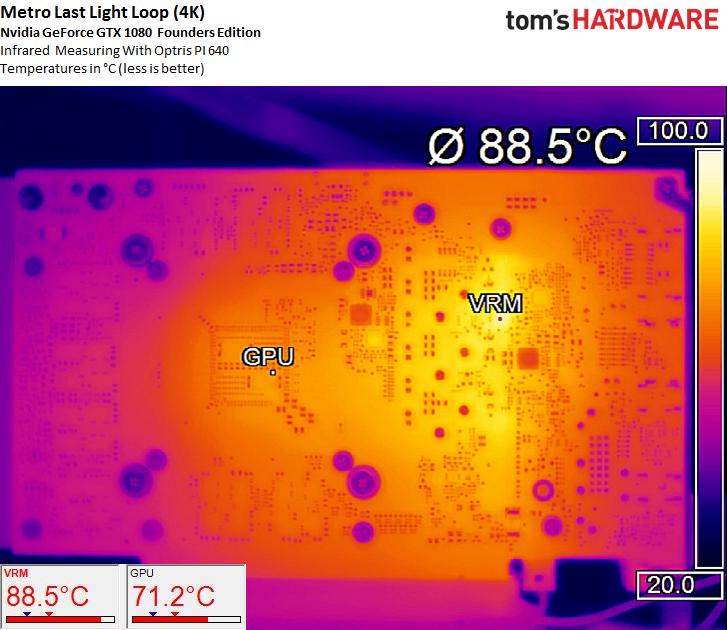
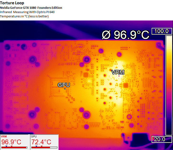
The infrared picture tells us that the cooling solution does its job well. All four of the voltage converter areas are in great shape as well.
During the stress test, the GPU’s three voltage converters reach 97 degrees Celsius, which is just within the acceptable range. Then again, nobody runs stress tests for hours, so this result is more theoretical, and not so practical, in nature.
Sound Results
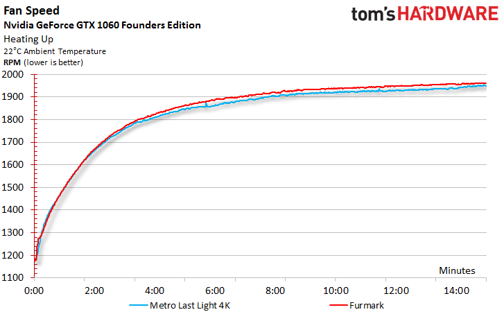
Next, we want to quantify just how loud the GeForce GTX 1060 gets under these conditions. The largest source of noise is generally the fan, so we look at that first. Its rotational speed takes a while to plateau, finally stabilizing after about 15 minutes. The two curves are almost on top of each other, which is again hardly surprising seeing that the temperatures the cooler deals with are almost identical as well.
At idle, we measure 31.4 dB(A). This is a good result that’s barely above the noise level encountered in a living room. The sound produced by Nvidia’s radial fan is noticeably more pleasant than that of AMD's reference Radeon RX 480. Nvidia's fan is a bit louder, though.
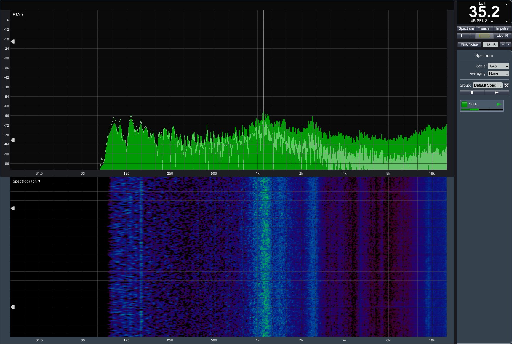
The good news continues with our gaming loop results. After reaching its maximum temperature, the GeForce GTX 1060 emits just 35.4 dB(A). Motor and bearing noises can’t really be heard above the relatively pleasant swooshing noise produced by the card. The sound isn't as low and growling as what we hear from AMD's competing offering. For more on that card, check out AMD Radeon RX 480 8GB Review.
Even a casual glance at this graph reveals that the majority of the GeForce GTX 1060’s operating noise comes from the fan blades and airflow. The voltage regulation circuitry doesn't contribute at all. This means that the DHE cooling solution performs well, doing its job quietly. Then again, it's not that big of a challenge to dissipate 120W.
Reasons to buy
Reasons to avoid
MORE: Nvidia GeForce GTX 1080 Roundup
MORE: Nvidia GeForce GTX 1070 Roundup
MORE: All Graphics Content
Current page: Nvidia GeForce GTX 1060 Founders Edition
Prev Page Benchmark Results Next Page EVGA GeForce GTX 1060 SC GamingGet Tom's Hardware's best news and in-depth reviews, straight to your inbox.

Igor Wallossek wrote a wide variety of hardware articles for Tom's Hardware, with a strong focus on technical analysis and in-depth reviews. His contributions have spanned a broad spectrum of PC components, including GPUs, CPUs, workstations, and PC builds. His insightful articles provide readers with detailed knowledge to make informed decisions in the ever-evolving tech landscape
-
Achaios @Igor: I really appreciate your articles. I have one small request: PLEASE consider adding benchmarks results from 3D MARK FIRESTRIKE so that we can compare your results with our GPU's. Really appreciated your "Das große Radeon RX480 Test-Roundup - Teil 1" too, though again, there are no 3D MARK FIRESTRIKE results.Reply -
bloodroses Darnit, the Zotac and Gigabyte mini models weren't covered. I was curious to see how those two compare vs. the EVGA model since I'm working with limited space inside my case.Reply -
agent88 I bought a retail MSI Geforce GTX 1060 Gaming X card last month and it was defaulted to OC mode by default. This is the same as the test version that the press received. Wondering if MSI is shipping this version to all consumers now or if I just got lucky with a "golden sample". Also, MSI provides both the MSI gaming app and afterburner software. The gaming app offers 1-click option to choose the OC mode. AReply -
shrapnel_indie Good to see a roundup... However, I think the 3GB and the 6GB belong in the same category as much as the RX-470 and RX-480 do. That is: they don't.Reply -
FritzEiv We're working on getting more cards in for all categories (1080, 1070, 1060), including from Asus, which is working on getting us cards. In fact, we'll have an update to our 1070 roundup shortly (2 new cards). And we're working on a 480 roundup as well.Reply -
mikeangs2004 Reply19457023 said:Darnit, the Zotac and Gigabyte mini models weren't covered. I was curious to see how those two compare vs. the EVGA model since I'm working with limited space inside my case.
they are kind of for the niche market just like in the days of low profile units -
Ancient1 Regarding the EVGA GTX 1060 SC :Reply
Could someone who disassemble it post the measurements ( WxHxL ) of the HEATPIPE ?? I plan on carving a Copper Heatsink, rather than Thermal Pads.
I am also thinking about HS for the memory etc , along the Pipe. But it will impact AirFlow and might degrade the HeatPipe efficiency as , to my knowledge, Heatpipe depends on temperature difference between the cooled GPU and the Heat Expelling (to the fins) areas of it.
Please post, Google will find it :)
Thanks in advance


