Nvidia GeForce GTX 1080 Pascal Review
Get Tom's Hardware's best news and in-depth reviews, straight to your inbox.
You are now subscribed
Your newsletter sign-up was successful
Disassembling GeForce GTX 1080 Founders Edition
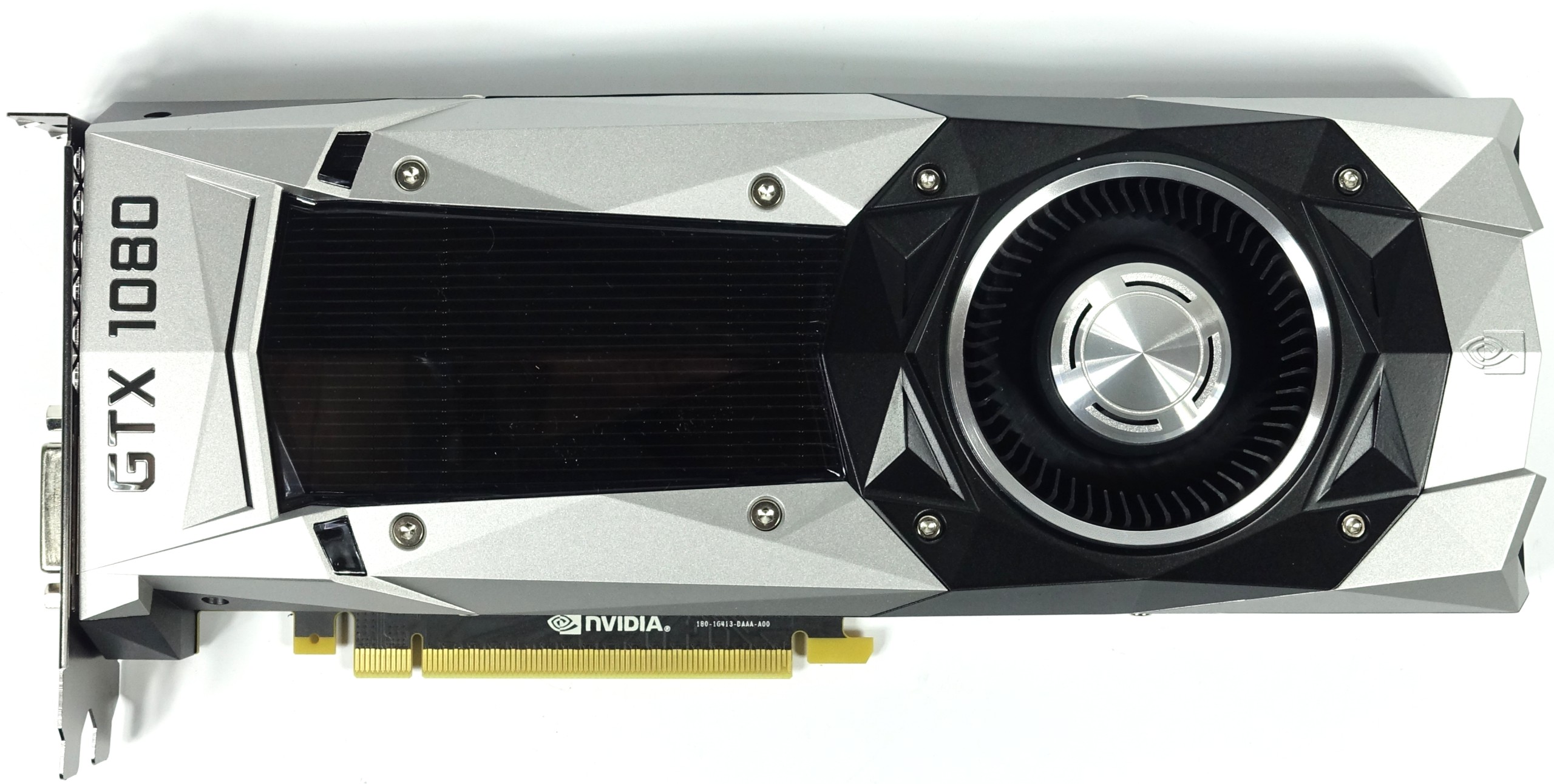
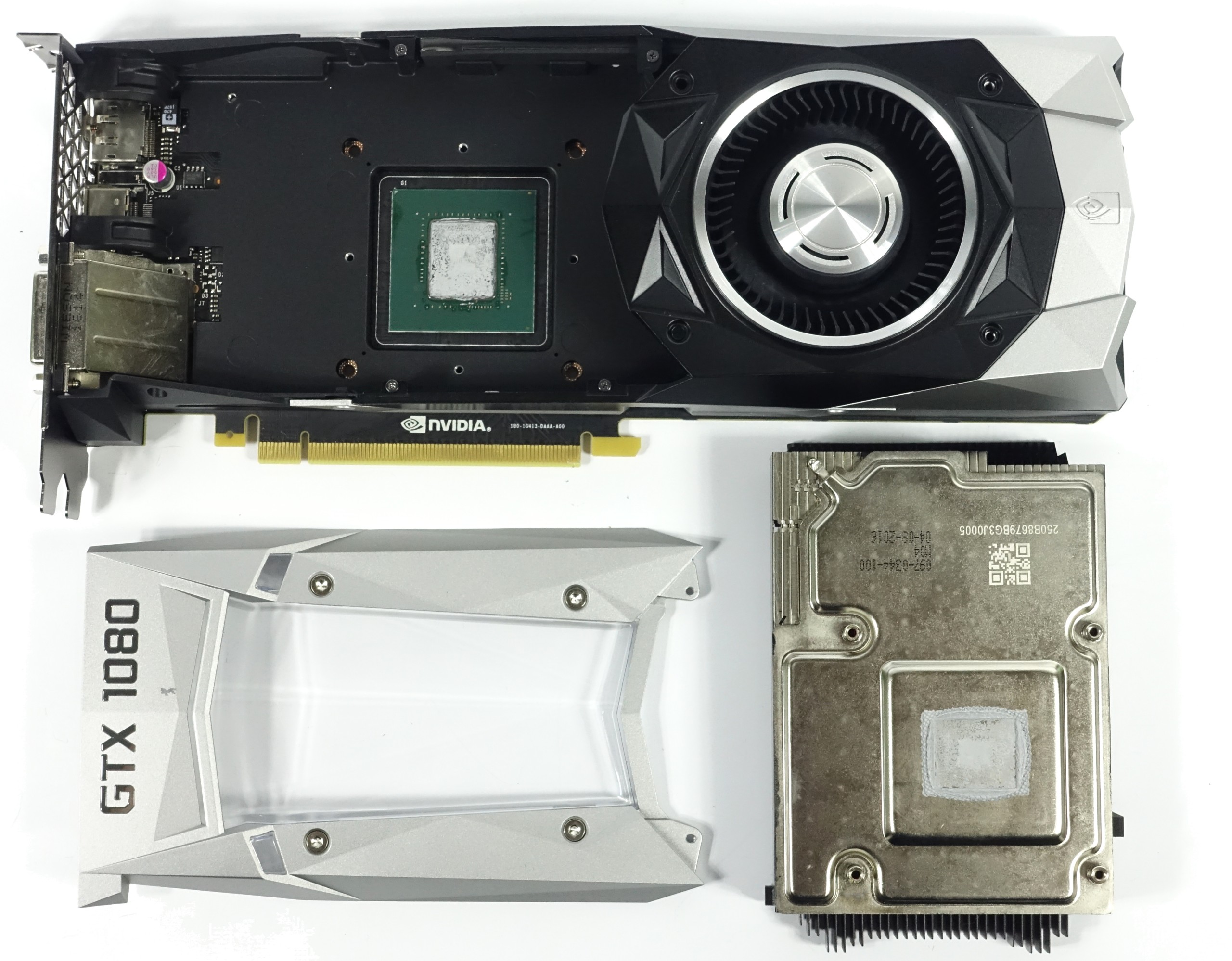
Nvidia is making changes to the way it refers to its own industrial design. Instead of using the word "reference," it calls its own version the Founders Edition. You'll notice that the GeForce GTX 1080's exterior is more angular this time around, though the cooling solution is still direct heat exhaust-based.
The card weighs in at 1020g and is 27cm long. It feels nice to the touch because the shroud doesn’t just look like it’s made of metal; it actually is (aluminum, to be exact). The matte silver parts get their color from lacquer, which means they'll scratch easily if you're not careful.
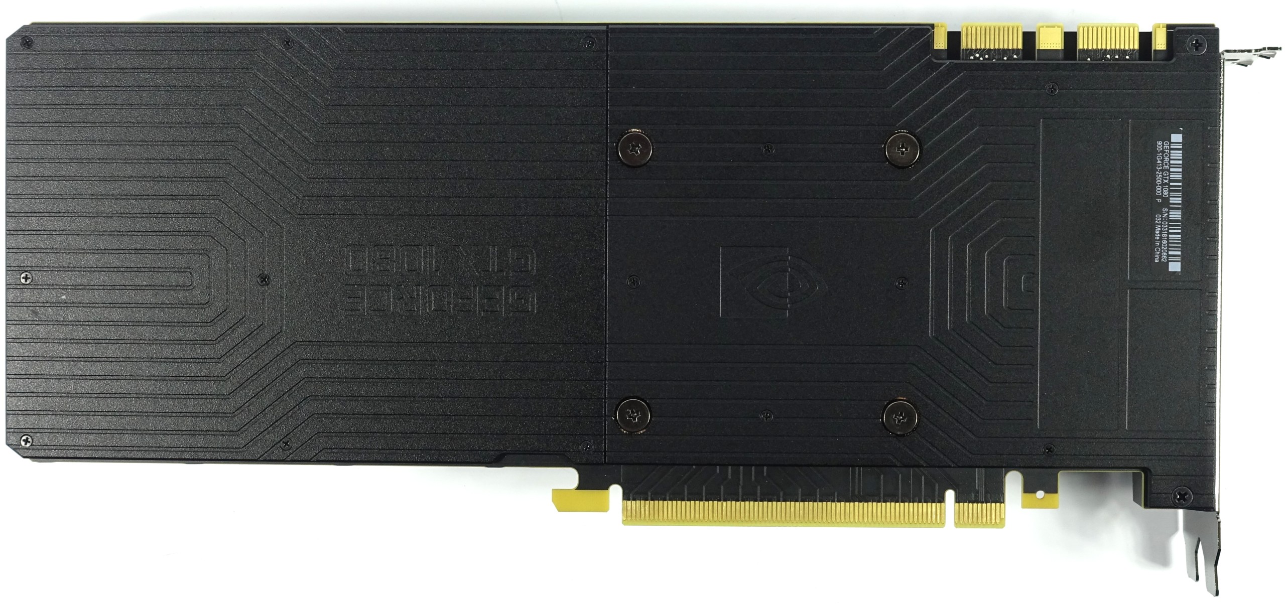
The backplate has two parts. Its only purpose is to make the graphics card look good. It doesn’t contribute to cooling. Later we'll determine if that was a good call. Nvidia actually recommends taking parts of the plate off when running in SLI to achieve better airflow between boards installed back to back.
Article continues belowThere’s nothing remarkable about the bottom of the card, though we did notice that parts of the black cover have a tendency to connect with motherboard components underneath, such as the chipset cooler and SATA ports.
The top of the 1080 is more interesting. There’s a single auxiliary eight-pin power connector, to start. Taking into account the graphics card’s official specs, along with the fact that it can draw up to 60W through the motherboard's 12V rail, this connector should be just enough for Nvidia's 180W TDP rating. Naturally, we'll take a closer look at how much power the graphics card actually draws, and if that leaves it with any reserves.
There are also two SLI connectors. Nvidia is introducing new high-bandwidth bridges to complement its Pascal-based cards, and we'll be going into more depth on that feature as well. In brief, though, SLI is only officially supported in two-way configurations moving forward, and both connectors are used to enable a dual-link interface between GPUs.
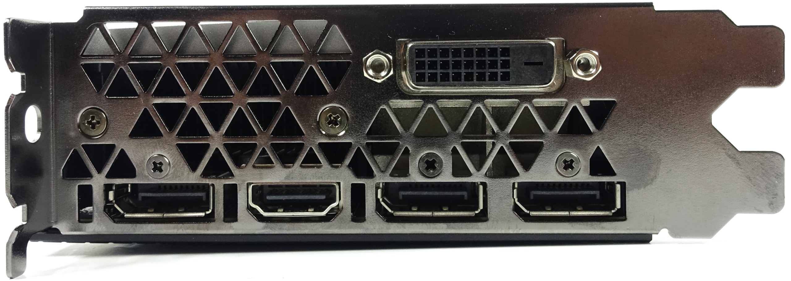
Three full-sized DisplayPort connectors dominate the I/O bracket. These are certified as DisplayPort 1.2, but are also supposed to be DisplayPort 1.3/1.4-ready (the display controller can handle those new standards, at least). There’s also an HDMI 2.0 connector and a dual-link DVI-D connector. Don't even bother looking for an analog signal.
Get Tom's Hardware's best news and in-depth reviews, straight to your inbox.
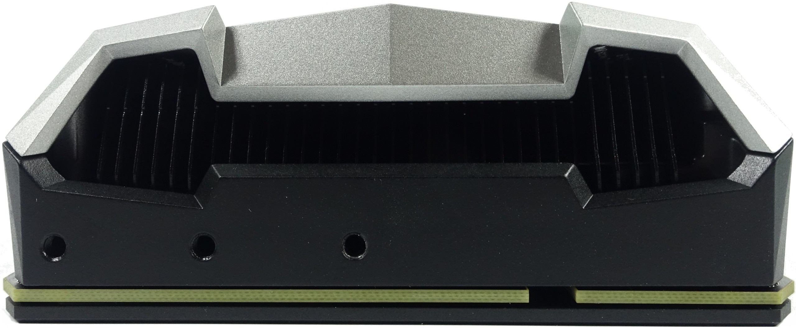
At the other end, there's a large opening for air and three threaded holes that can be used to secure the card.
Cooler Design And Power Supply
After our careful examination of the card’s exterior, it’s time to take a look underneath its aluminum cover. This is a more complicated undertaking than you might assume. With everything removed, there are 51 individual parts, including screws, sitting on our test bench. Removing the fan would yield another 12.
Nvidia finally returned to a true vapor chamber solution, which is held in place atop the GPU by four screws attached to the board, next to the GPU.
The centrifugal fan should already be familiar to you. In true direct heat exhaust fashion, it sucks air in, blows it across the cooler's fins and exhausts it out the back of your case. The cover, which doubles as a frame, doesn’t just stabilize the card but also helps cool components like the voltage converters and memory modules.
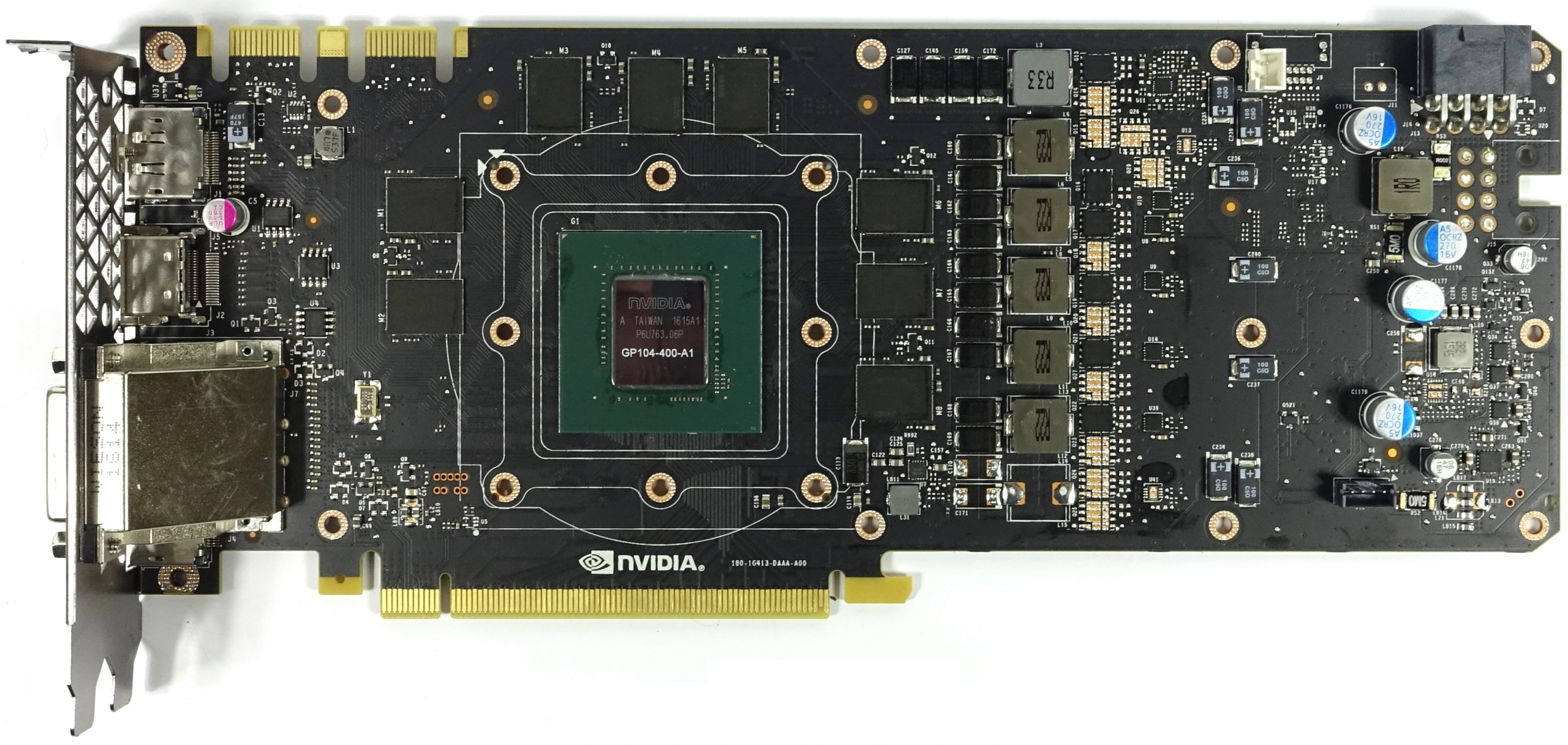
Our hard work is rewarded with a clear and unobstructed view of the PCA. Nvidia is using a six-phase design, which is different from prior solutions. Five phases service the GPU’s complex power supply, and the remaining phase provides a constant supply for the GDDR5X memory.
We also see that there is room for another phase, though the space for it is left empty.
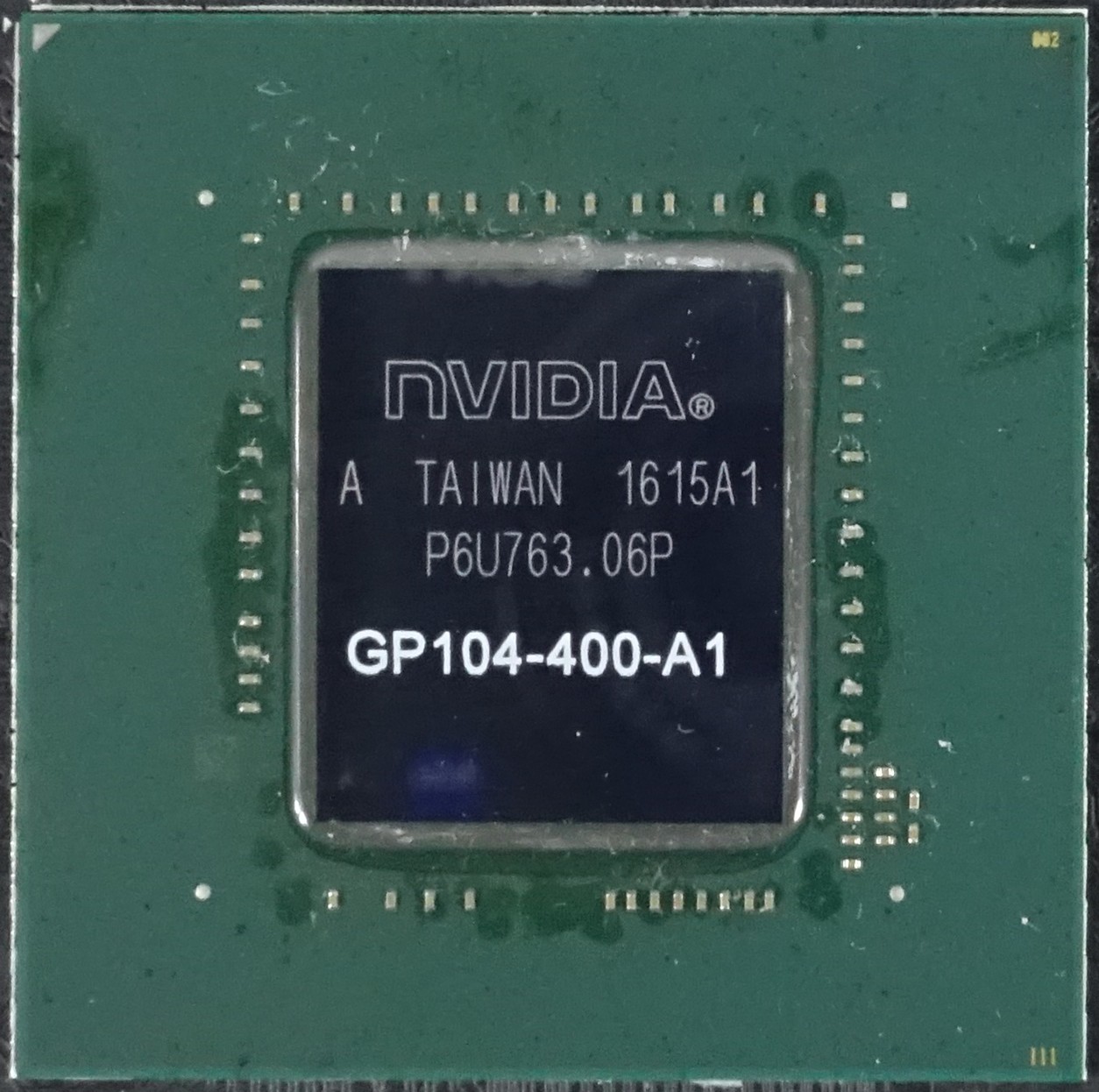
GP104 is a lot smaller than its predecessor at 314mm². It’s interesting to see the circuits on the different board layers around the GPU. The signal pathways need to be shorter and laid out precisely due to the high frequencies. The tight tolerances involved in getting this right will probably result in a bit of a wait before we see the first designs from Nvidia's board partners.
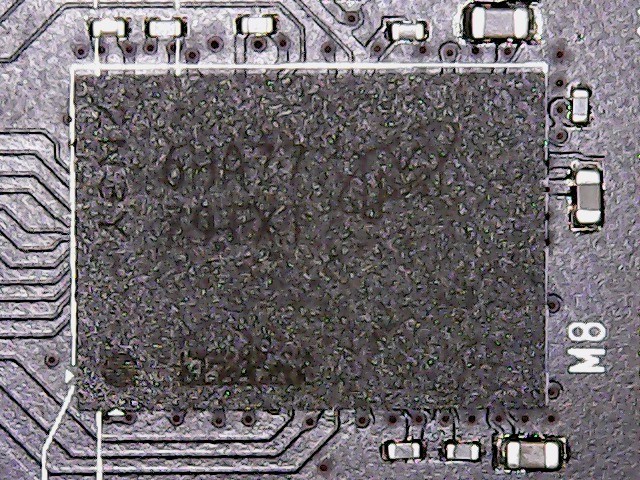
The memory is of course different as well; it's 6HA77, which is Micron's GDDR5X. It entered mass production recently, as leaked pictures of Nvidia’s new graphics card had 6GA77 instead.
A total of eight memory packages are connected to an aggregate 256-bit memory bus through 32-bit controllers. Clocked at 1251MHz, this yields a 10 Gb/s data rate capable of up to 320 GB/s.
Micron's GDDR5X modules employ 170-pin packaging instead of GDDR5's 190 pins. The modules are also a bit smaller at 14x10mm instead of 14x12mm. That means we’re looking at higher-density modules, necessitating better cooling.
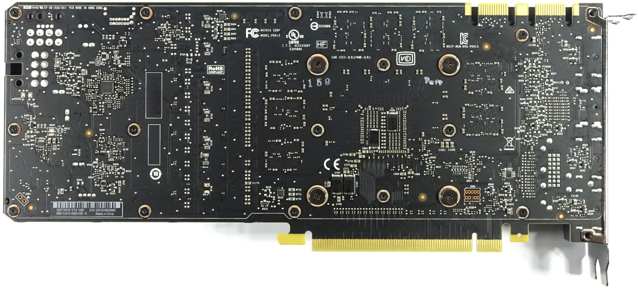
Flipping the card over to look at its back, we can't help but notice the empty space for a second power connector. This should give Nvidia’s partners some flexibility to either feed their boards more power or move the connector to a rear-facing orientation.
Notably, there’s also a gap in the board that allows the power connector to be turned by 180 degrees.
Capacitors are located directly underneath the GPU to smooth out any spikes. The PWM controller is on this side of the board as well (it was on the front previously). Again, that gives Nvidia's partners some freedom to add their own power boards with different PWM controllers.
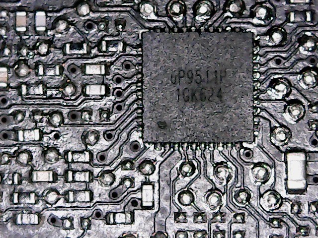
Let’s get back to the voltage regulator's PWM controller, though. Nvidia’s GPU Boost 3.0 has a new set of voltage regulation requirements, resulting in significant changes. We would have expected a controller like International Rectifier's IR3536A to be paired with a pure 5+1-phase design. But that's not the case. A µP9511P is used instead, which is bad news for anyone who likes to overclock, since the interface and protocol used by tools such as MSI Afterburner and Gigabyte’s OC Guru won't work with this card. The change to a new controller, which isn’t very well documented at this point, is probably due to technical considerations.
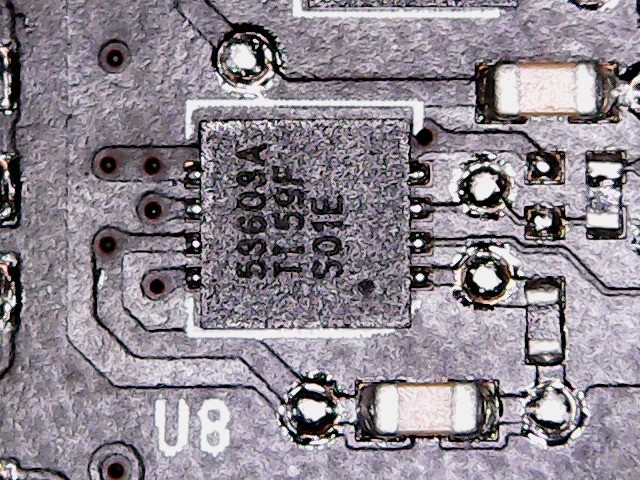
Nvidia uses solid MOSFET gate drivers with the 53603A for PWM control of the power MOSFETs, since the PWM controller can’t directly address individual voltage converter phases. The circuit layout is nice and tidy though, which is a nice change from some of the designs we've seen.
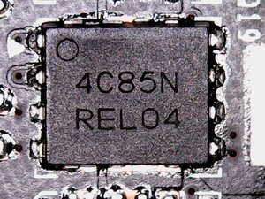
There are different types of MOSFETs here. The 4C85N is a fairly resilient dual-channel MOSFET in the DC/DC voltage converter area. It services all of the power supply’s six phases, and has enough electrical and thermal reserves to take whatever the reference design throws at it.
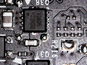
It’ll be interesting to see how Nvidia’s GPU Boost 3.0 technology and the voltage regulation’s modified layout affect power consumption. You can bet we'll be measuring all of that shortly.
Current page: Disassembling GeForce GTX 1080 Founders Edition
Prev Page Meet GP104 Next Page Simultaneous Multi-Projection And Async Compute-
JeanLuc Chris, were you invited to the Nvidia press event in Texas?Reply
About time we saw some cards based of a new process, it seemed like we were going to be stuck on 28nm for the rest of time.
As normal Nvidia is creaming it up in DX11 but DX12 performance does look ominous IMO, there's not enough gain over the previous generation and makes me think AMD new Polaris cards might dominate when it comes to DX12. -
slimreaper Could you run an Otoy octane bench? This really could change the motion graphics industry!?Reply
-
F-minus Seriously I have to ask, did nvidia instruct every single reviewer to bench the 1080 against stock maxwell cards? Cause i'd like to see real world scenarios with an OCed 980Ti, because nobody runs stock or even buys stock, if you can even buy stock 980Tis.Reply -
cknobman Nice results but honestly they dont blow me away.Reply
In fact, I think Nvidia left the door open for AMD to take control of the high end market later this year.
And fix the friggin power consumption charts, you went with about the worst possible way to show them. -
FormatC Stock 1080 vs. stock 980 Ti :)Reply
Both cards can be oc'ed and if you have a real custom 1080 in your hand, the oc'ed 980 Ti looks in direct comparison to an oc'ed 1080 worse than the stock card in this review to the other stock card. :) -
Gungar @F-minus, i saw the same thing. The gtx 980Ti overclocks way better thn 1080, i am pretty sure OC vs OC, there is nearly no performance difference. (disappointing)Reply -
toddybody Reply@F-minus, i saw the same thing. The gtx 980Ti overclocks way better thn 1080, i am pretty sure OC vs OC, there is nearly no performance difference. (disappointing)
LOL. My 980ti doesnt hit 2.2Ghz on air. We need to wait for more benchmarks...I'd like to see the G1 980ti against a similar 1080. -
F-minus Exactly, but it seems like nvidia instructed every single outlet to bench the Reference 1080 only against stock Maxwell cards, which is honestly <Mod Edit> - pardon. I bet an OCed 980Ti would come super close to the stock 1080, which at that point makes me wonder why even upgrade now, sure you can push the 1080 too, but I'd wait for a price drop or at least the supposed cheaper AIB cards.Reply -
FormatC I have a handpicked Gigabyte GTX 980 Ti Xtreme Gaming Waterforce at 1.65 Ghz in one of my rigs, it's slower.Reply
