NVIDIA GeForceFX: Brute Force Attack Against the King
Get Tom's Hardware's best news and in-depth reviews, straight to your inbox.
You are now subscribed
Your newsletter sign-up was successful
The GeForceFX GPU, Continued
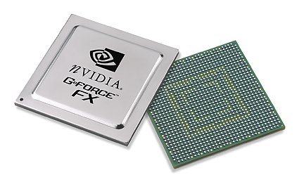
The GeForceFX chip is the first consumer-level graphics chip to be manufactured in the 0.13µ process. This lets NVIDIA clock the chip, which is produced in a flip-chip design, to a breathtaking 500 MHz. With 125 million transistors, the GeForceFX GPU is more than twice the size of a Pentium 4 CPU (55 million transistors). High power consumption aside (just like ATI's R300 cards R9700 and R9500 the GeForceFX requires an additional power supply), this generates a considerable amount of heat and therefore requires extensive cooling.
Compared to the GeForce4 Ti, the number of pixel pipes has been increased from four to eight. This allows the FX to process eight pixels per clock cycle with a texture. However, the GeForce4 GPU could calculate two textures per pipe, while the FX pipes can only process one. With multitexturing, the advantage is again reduced.
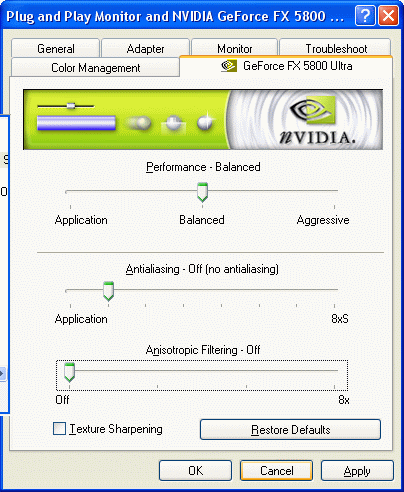
NVIDIA also re-worked the filtering. The performance of the FX in tri-linear and anisotropic filtering modes has increased considerably. The chip now decides internally which filter level to use. Anti-aliasing has also been optimized and is now called "Intellisample" with the FX. Newcomers in the FX are anti-aliasing modes 6X and 8X under Direct 3D.
Article continues belowGet Tom's Hardware's best news and in-depth reviews, straight to your inbox.
Current page: The GeForceFX GPU, Continued
Prev Page Introduction Next Page The GeForceFX GPU, Continued
