


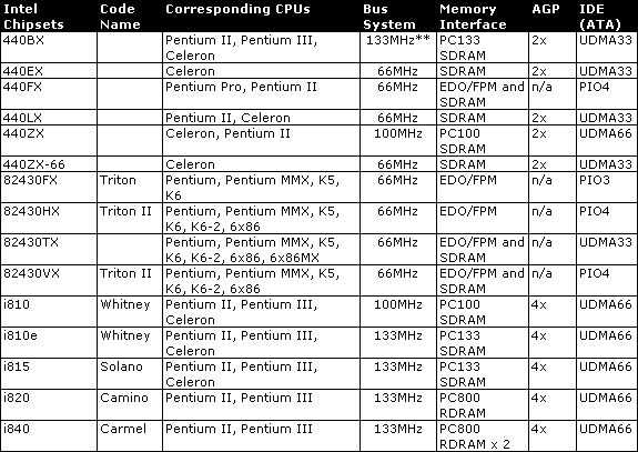
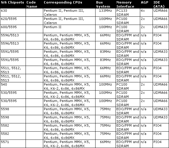
Chipsets And Corresponding Processors

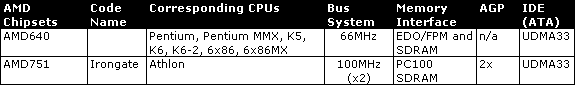
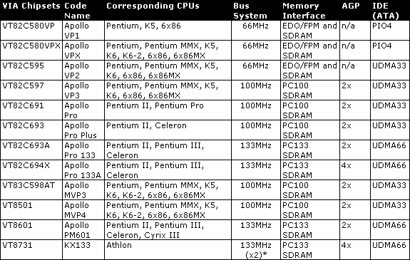
* KX133 Chipset: The FSB of current Athlons (K7) should not exceed 100 MHz (x2 or Double Data Rate). The clock rate of 133 MHz for the memory interface is produced by an addition of FSB and PCI clock.
** beyond 'official' specification, AGP divisor is locked at 2/3 of the system bus, i.e. the AGP bus runs at 88.8 MHz when the FSB is 133 MHz, default would be 66.6 MHz Bus System, also referred to as Front Side Bus (FSB)
Swipe to scroll horizontally
| Row 0 - Cell 0 | |
| Memory Interface | |
| EDO | Extended DataOut or Hyperpage Mode of Asynchronous DRAM |
| FPM | Fast Page Mode (memory without Column Address Setup Time) |
| SDR | Single Data Rate |
| DDR | Double Data Rate |
| SDRAM | Synchronous Dynamic Random Access Memory |
| RDRAM | Direct Rambus Random Access Memory |
| PC100 | Clock is max. 100 MHz x 1 x 8 Byte equals to max. 0.8 GByte/s data throughput, short latencies |
| PC133 | Clock is max. 133 MHz x 1 x 8 Byte equals to max. 1.1 GByte/s data throughput, short latencies |
| PC266 | Clock is max. 133 MHz x 2 x 8 Byte equals to max. 2.2 GByte/s data throughput, short latencies |
| PC600 | Clock is max. 266 MHz x 2 x 2 Byte equals to max. 1.1 GByte/s data throughput, long latencies |
| PC700 | Clock is max. 356 MHz x 2 x 2 Byte equals to max. 1.4 GByte/s data throughput, long latencies |
| PC800 | Clock is max. 400 MHz x 2 x 2 Byte equals to max. 1.6 GByte/s data throughput, long latencies |
| AGP Bandwidth | |
| n/a | in this case only PCI slots (132 MByte/s) are supported |
| AGP 1X | dedicated graphics card bus with a max. transfer rate of 266 MByte/s |
| AGP 2X | dedicated graphics card bus with a max. transfer rate of 528 MByte/s |
| AGP 4X | dedicated graphics card bus with a max. transfer rate of 1 GByte/s |
| IDE (ATA) Interface | |
| UDMA66 | max. HDD transfer rate of 66.6 MByte/s using bus mastering (minimizes CPU utilisation) |
| UDMA33 | max. HDD transfer rate of 33.3 MByte/s using bus mastering (minimizes CPU utilisation) |
| PIO4 | max. HDD transfer rate of 16.6 MByte/s not using bus mastering (leads to strong CPU utilisation) |
TOPICS
