AMD Radeon HD 6870 And 6850: Is Barts A Step Forward?
Radeon HD 6800-Series Architechture
In the past, we've seen a refresh to the Radeon lineup on a yearly basis, accompanied by a process improvement. But the Radeon HD 6800-series is being delivered using the same TSMC-based 40 nm node first used in April of 2009 to manufacture the Radeon HD 4770. Forty nanometer technology was also deployed across the Radeon HD 5000-series. And now it's being recycled for the Radeon HD 6800s. According to Eric Demers, CTO of AMD's GPU division, sticking with the established process made more fiscal sense this time around. Based on yields, the company essentially had to decide between two 32 nm processors or three 40 nm GPUs at a similar cost. From here, though, we're expecting AMD to skip 32 nm and transition straight to 28 nm manufacturing.
With no process improvement of which to speak, making Barts a worthwhile step forward becomes a more challenging task for the GPU architects.
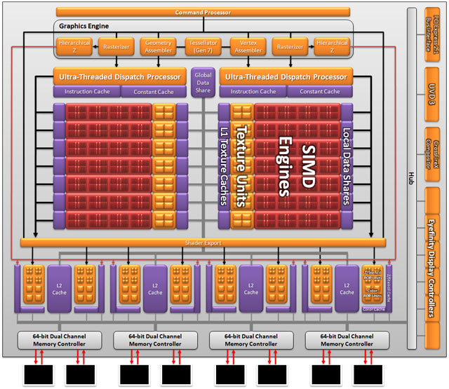
We expect that you'll have a tough time telling the difference between AMD's Radeon 5800- and 6800-series GPUs on this schematic. In fact, if you squint and count the SIMD engines, the new Barts GPU looks notably weaker than the Radeon HD 5870's Cypress. Of course, performance is all in the numbers:
| Header Cell - Column 0 | Radeon HD 5850 | Radeon HD 5830 | Radeon HD 6870 | Radeon HD 6850 |
|---|---|---|---|---|
| Shader Processors: | 1440 | 1120 | 1120 | 960 |
| Texture Units: | 72 | 56 | 56 | 48 |
| Color ROPs: | 32 | 16 | 32 | 32 |
| Core Clock: | 725 MHz | 800 MHz | 900 MHz | 775 MHz |
| GDDR5 Memory Clock: | 1000 MHz | 1000 MHz | 1050 MHz | 1000 MHz |
| Memory Bus: | 256-bit | 256-bit | 256-bit | 256-bit |
| Memory Bandwidth (GB/s): | 128 | 128 | 134.4 | 128 |
| Die Size: | 334 mm2 | 334 mm2 | 255 mm2 | 255 mm2 |
| Transistors (billion): | 2.15 | 2.15 | 1.7 | 1.7 |
| Maximum Power: | 151 W | 175 W | 151 W | 127 W |
| Idle Power: | 27 W | 25 W | 19 W | 19 W |
The Radeon HD 6870 employs 14 SIMD engines, each hosting four texture units and 16 stream processors. Each stream processor is armed with five ALUs (AMD calls these stream cores). As a result, this GPU has a total 1120 stream cores and 56 texture units. The GPU channels output through four render back-ends, each containing eight color ROP units, resulting in an effective total of 32 ROPs. Four 64-bit memory controllers yield a 256-bit aggregate memory interface.
If any of this sounds familiar, it’s probably because, from a raw specifications standpoint, the new Radeon HD 6870 is essentially a Radeon HD 5830 with twice the render back-ends. Or, viewed differently, the Radeon HD 6870 has the same back-end as the 5870, just fewer shader cores. When the Radeon HD 5830 was released, we lamented the merciless halving of ROPs, and in a way, the Radeon HD 6870 shows us what the 5830 could have been.
But there’s one more critical component to performance, and that’s clock rate. Despite the re-use of 40 nm manufacturing, at 900 MHz, the less-complex Barts GPU runs much faster than the 5830, or even the 5850. This means geometry throughput is almost 25% higher than the 725 MHz Radeon HD 5850 because it’s limited to one primitive and one vertex per clock cycle. At the same time, the 6870’s texture unit and ALU deficit (compared to the 5850) is offset by a higher core clock, resulting in roughly the same overall performance.
At the end of the day, this means the Radeon HD 6870 performs a little better than the Radeon HD 5850, but does it with about 25% less silicon, purportedly reducing idle power and overall cost--two definite benefits for the end user. The Radeon HD 6870's memory runs at 1050 MHz, slightly faster than the 5850's 1000 MHz. The MSRP of the Radeon HD 6870 is $240, a bit less than the Radeon HD 5850, which still sells online for $260 and up (though rebates take it lower).
Get Tom's Hardware's best news and in-depth reviews, straight to your inbox.
The second product based on AMD's RV870 GPU is the Radeon HD 6850. The only difference here is that two of the GPU’s 14 SIMDs are disabled, resulting in 12 SIMDs with a total 960 stream cores and 48 texture units. The core clock drops to 775 MHz, but all of the render back-ends are fortunately left intact. The resulting performance should be notably faster than Radeon HD 5830. AMD’s suggested retail price of the Radeon HD 6850 is $180, and while Radeon HD 5830 cards can sometimes be found for that price, the majority of them are in the $200 range. More threatening to the Radeon HD 6850 will be an onslaught from Nvidia, which we'll also dissect in more depth.
Tessellation
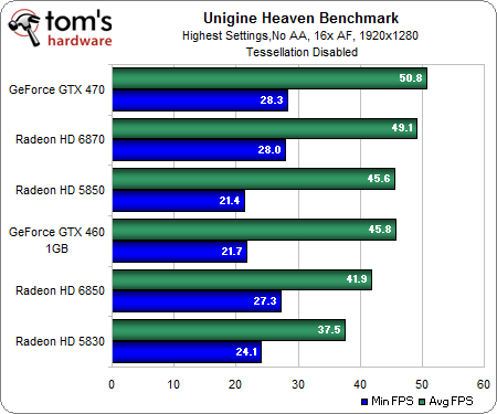
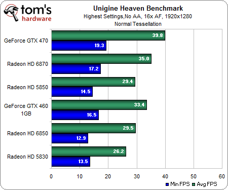
On the surface, both Barts-based SKUs appear to be (at least architecturally) derived wholly from Cypress. But AMD's engineers assure us that notable improvements have been made, and features added. Perhaps the highest-profile performance-adder is an enhanced tessellation unit. According to the company, improved thread management and buffering yields between 1.5 and 2x performance in what it considers the most important (real-world) range, below 14 tessellation factors. We can see the result of this in the Unigine Heaven benchmark:
The first chart shows the benchmark results with no tessellation applied, and the second demonstrates results with the normal tessellation level enabled. When tessellation is used, we can see the Radeon HD 6850 reach Radeon HD 5850-class performance, and the Radeon HD 6870 leaves the other Radeons behind.
This is a particularly sensitive subject for AMD. When Nvidia launched GF100, it went straight for AMD's throat, claiming the single fixed-function tessellation unit would not scale well. Instead, Nvidia advocated its Polymorph Engine, present on each of its architecture's Shader Multiprocessors. Parallelizing geometry, it claimed, was the key to adding the next level of realism. AMD counters that geometry is actually better-addressed through its single unit, and that its approach is much more efficient.
At the end of the day, Nvidia still outperforms AMD in synthetic measures of tessellation. But we still haven't seen a game capable of coming anywhere close to giving Nvidia an advantage due to its geometric processing potential. From what we hear, Nvidia took Ubisoft to bed, and the result, HAWX 2, employs what amounts to a worst-case geometry scenario for AMD. That might turn out to be the first example of Nvidia's advantage, even if it was sponsored. It remains to be seen whether AMD can get the developer to add a slider for geometry detail. At least, that's the current plan, according to company representatives.
Current page: Radeon HD 6800-Series Architechture
Prev Page The New Radeon HD 6000 Family Next Page Stereoscopic 3D With AMD’s HD3DDon Woligroski was a former senior hardware editor for Tom's Hardware. He has covered a wide range of PC hardware topics, including CPUs, GPUs, system building, and emerging technologies.
-
SteelCity1981 Yeah I agree. I don't get AMD's marketing on the 6000 series. One would think that the 6870 would obv performan better then the 5870 at first glance but instead it yelds less performance then the 5870. That just doesn't make any sense from a consumor standpoint.Reply -
TheRockMonsi I like where AMD is going with the 6000 series, not so much with naming, but pretty much everything else about it. Can't wait for the 6900's, those are going to be beasts!!!!!Reply -
Poisoner I think AMD did a great job with these cards. Its just sick at what performance you can get for 200 bucks.Reply -
duk3 Nice benchmark suite!Reply
I am looking forward to the 6900 series and 22nm gpus later on for some real performance improvements. -
takeapieandrun Not exactly powerhouses, but I do believe they will be great for market competition.Reply -
forces nice but... where is Crysis!!!? they can play Crysis i know but how well can they play it? everyone has Crysis and have played Crysis and will play it... :(, its a nice game to compare perfomance...Reply


