


The Ampere architecture will power the GeForce RTX 3090, GeForce RTX 3080, GeForce RTX 3070, and other upcoming Nvidia GPUs. It represents the next major upgrade from Team Green and promises a massive leap in performance. Based on current details (the cards come out later this month and in October for the 3070), these GPUs should easily move to the top of our GPU hierarchy, and knock a few of the best graphics cards down a peg or two. Let's get into the details of what we know about the Ampere architecture, including specifications, features, and other performance enhancements.
[Note: We've updated some of the information on the CUDA cores and how it effects performance, provided accurate die size and transistor counts, and additional details on DLSS 2.1 and ray tracing improvements.]
The Ampere architecture marks an important inflection point for Nvidia. It's the company's first 7nm GPU, or 8nm for the consumer parts. Either way, the process shrink allows for significantly more transistors packed into a smaller area than before. It's also the second generation of consumer ray tracing and third generation deep learning hardware. The smaller process provides a great opportunity for Nvidia to radically improve on the previous RTX 20-series hardware and technologies.
We know the Ampere architecture will find its way into upcoming GeForce RTX 3090, RTX 3080, and RTX 3070 graphics cards, and we expect to see RTX 3060 and RTX 3050 next year. It's also part of the Nvidia A100 data center GPUs, which are a completely separate category of hardware. Here we'll break down both the consumer and data center variations of the Ampere architecture and dig into some of the differences.
The launch of Nvidia's Ampere GPUs feels like a blend of 2016's Pascal and 2018's Turing GPus. Nvidia CEO Jensen Huang unveiled the data center focused A100 on May 14, giving us our first official taste of what's to come, but the A100 isn't designed for GeForce cards. It's the replacement for the Volta GV100 (which replaced the GP100). The consumer models have a different feature set, powered by separate GPUs like the GA102, GA104, and so on. The consumer cards also use GDDR6X/GDDR6, where the A100 uses HBM2.

Besides the underlying GPU architecture, Nvidia has revamped the core graphics card design, with a heavy focus on cooling and power. As an Nvidia video notes, "Whenever we talk about GPU performance, it all comes from the more power you can give and can dissipate, the more performance you can get." A reworked cooling solution, fans, and PCB (printed circuit board) are all part of improving the overall performance story of Nvidia's Ampere GPUs. Of course, third party designs are free to deviate from Nvidia's designs.
With the shift from TSMC's 12nm FinFET node to TSMC N7 and Samsung 8N, many expected Ampere to deliver better performance at lower power levels. Instead, Nvidia is taking all the extra transistors and efficiency and simply offering more, at least at the top of the product stack. GA100 for example has 54 billion transistors and an 826mm square die size. That's a massive 156% increase in transistor count from the GV100, while the die size is only 1.3% larger. The consumer GPUs also increase in transistor counts while greatly reducing die sizes.
While 7nm/8nm does allow for better efficiency at the same performance, it also allows for much higher performance at the same power. Nvidia is taking the middle route and offering even more performance at still higher power levels. The V100 was a 300W part for the data center model, and the new Nvidia A100 pushes that to 400W. We see the same on the consumer models. GeForce RTX 2080 Ti was a 250/260W part, and the Titan RTX was a 280W part. The RTX 3090 comes with an all-time high TDP for a single GPU of 350W (that doesn't count the A100, obviously), while the RTX 3080 has a 320W TDP.
What does that mean to the end users? Besides potentially requiring a power supply upgrade, and the use of a 12-pin power connector on Nvidia's own models, it means a metric truckload of performance. It's the largest single generation jump in performance I can recall seeing from Nvidia. Combined with the architectural updates, which we'll get to in a moment, Nvidia says the RTX 3080 has double the performance of the RTX 2080. And if those workloads include ray tracing and/or DLSS, the gulf might be even wider.
Thankfully, depending on how you want to compare pricing, pricing isn't going to be significantly worse than the previous generation GPUs. The GeForce RTX 3090 is set to debut at $1,499, which is a record for a single-GPU GeForce card, effectively replacing the Titan family. The RTX 3080 meanwhile costs $699, and the RTX 3070 will launch at $499, keeping the same pricing as the previous generation RTX 2080 Super and RTX 2070 Super. Does the Ampere architecture justify the pricing? We'll have to wait a bit longer to actually test the hardware ourselves, but the specs at least look extremely promising.

Let's also tackle the efficiency question quickly. At one point in his presentation, Jensen said that Ampere delivers 1.9X the performance per watt as Turing. That sounds impressive, but that appears to be more of a theoretical performance uplift rather than what we'll see on the initial slate of GPUs.
Take the RTX 3080 as an example. It has a 320W TDP, which is nearly 50% more than the 215W TDP of the RTX 2080. Even if it really is double the performance of the RTX 2080, that's still only a 35% improvement in performance per watt.
Nvidia gets the 1.9X figure not from fps/W, but rather by looking at the amount of power required to achieve the same performance level as Turing. If you take a Turing GPU and limit performance to 60 fps in some unspecified game, and do the same with Ampere, Nvidia claims Ampere would use 47% less power.
That's not all that surprising. We've seen power limited GPU designs for a long time in laptops. The RTX 2080 laptops for example can theoretically clock nearly as high as the desktop parts, but they're restricted to a much lower power level, which means actual clocks and performance are lower. A 10% reduction in performance can often deliver a 30% gain in efficiency when you near the limits of a design.
AMD's R9 Nano was another example of how badly efficiency decreases at the limit of power and voltage. The R9 Fury X was a 275W TDP part with 4096 shaders clocked at 1050 MHz. R9 Nano took the same 4096 shaders but clocked them at a maximum of 1000 MHz, and applied a 175W TDP limit. Performance was usually closer to 925MHz in practice, but still at one third less power.

Nvidia Ampere Architecture Specifications
Along with the GA100 for data center use, Nvidia has at least three other Ampere GPUs slated to launch in 2020. There will potentially be as many as three additional Ampere solutions during the coming year, though those are as yet unconfirmed (and not in this table). Here's the high-level overview.
| GPU | GA100 | GA102 | GA102 | GA104 |
| Graphics Card | Nvidia A100 | GeForce RTX 3090 | GeForce RTX 3080 | GeForce RTX 3070 |
| Process (nm) | TSMC N7 | Samsung 8N | Samsung 8N | Samsung 8N |
| Transistors (billion) | 54 | 28.3 | 28.3 | 17.4 |
| Die Size (mm^2) | 826 | 628.4 | 628.4 | 392.5 |
| GPC Configuration | 8x16 | 7x12 | 6x12 | 6x8 |
| SMs | 108 | 82 | 68 | 46 |
| CUDA Cores | 6912 | 10496 | 8704 | 5888 |
| RT Cores | None | 82 | 68 | 46 |
| Tensor Cores | 432 | 328 | 272 | 184 |
| Boost Clock (MHz) | 1410 | 1700 | 1710 | 1730 |
| VRAM Speed (Gbps) | 2.43 | 19.5 (GDDR6X) | 19 (GDDR6X) | 14 (GDDR6) |
| VRAM (GB) | 40 (48 max) | 24 | 10 | 8 |
| Bus Width | 5120 (6144 max) | 384 | 320 | 256 |
| ROPs | 128 | 112 | 96 | 96 |
| TMUs | 864 | 656 | 544 | 368 |
| GFLOPS FP32 | 19492 | 35686 | 29768 | 20372 |
| RT TFLOPS | N/A | 69 | 58 | 40 |
| Tensor TFLOPS FP16 (sparsity) | 312 (628) | 143 (285) | 119 (238) | 81 (163) |
| Bandwidth (GB/s) | 1555 | 936 | 760 | 448 |
| TBP (watts) | 400 (250 PCIe) | 350 | 320 | 220 |
| Launch Date | May 2020 | September 24, 2020 | September 17, 2020 | October 15, 2020 |
| Launch Price | $199K for DXG A100 (with 8xA100) | $1,499 | $699 | $499 |
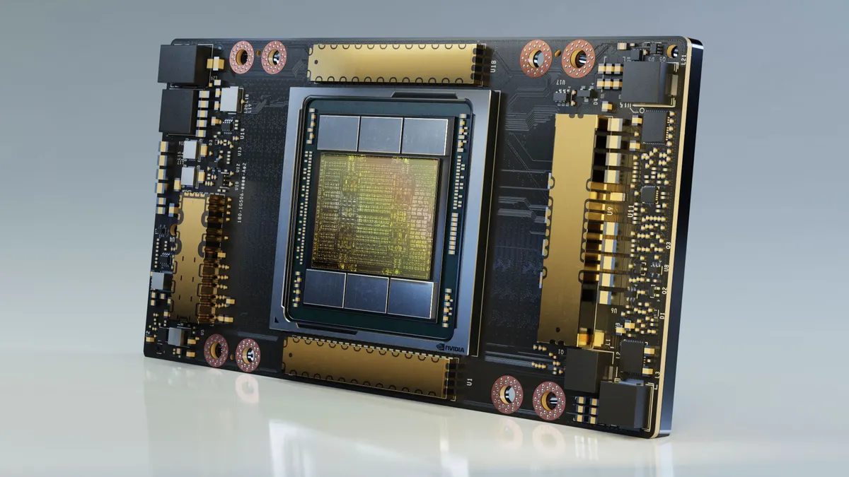
The biggest and baddest GPU is the A100. It has up to 128 SMs and six HBM2 stacks of 8GB each, of which only 108 SMs and five HBM2 stacks are currently enabled in the Nvidia A100. Future variations could have the full GPU and RAM configuration. However, the GA100 isn't going to be a consumer part, just like the GP100 and GV100 before it were only for data center and workstation use. Without ray tracing hardware, the GA100 isn't remotely viable as a GeForce card, never mind the cost of the massive die, HBM2, and silicon interposer.

Stepping down to the consumer models, Nvidia makes some big changes. Nvidia apparently doubled the number of FP32 CUDA cores per SM, which results in huge gains in shader performance. With the GA102, Nvidia has a total of seven GPC clusters, each with 12 SMs, giving a maximum configuration of 84 SMs. Of these, 82 are enabled in the RTX 3090 while the RTX 3080 only has 68 enabled. The HBM2 and silicon interposer are also gone, replaced by 24 GDDR6X chips, each running on a 16-bit half-width interface for the 3090, or 10 GDDR6X chips running on a 32-bit interface for the 3080.
With the doubled CUDA cores per SM, that equates to 10496 CUDA cores, with two FP64 capable CUDA cores per SM. In other words, FP64 performance is 1/64 the FP32 performance. Nvidia strips out the remaining FP64 functionality, and in its place adds 2nd generation RT cores. There are also four 3rd gen tensor cores, each of which is four times the throughput per clock of the previous gen Turing tensor cores.
The boost clock of 1700 MHz gives a potential 35.7 TFLOPS of FP32 compute performance, and the 19.5 Gbps GDDR6X delivers 936 GBps of bandwidth. In case that's not clear, potentially the RTX 3090 will have more than double the performance of the RTX 2080 Ti.
Considering the RTX 3090 is very nearly a full GA102 chip, there's not much room for anything faster right now. Could there be a future Titan card with a fully enabled GA102? Absolutely, but it would only be 2.4% faster at the same clocks as the 3090. Maybe 21 Gbps memory would help, but realistically we don't see Nvidia doing a Titan card for Ampere. Instead, the RTX 3090 is an extreme performance consumer-focused card, and it's now open for third parties to create custom designs (unlike the Titan cards of previous generations).

There's more to it than a simple doubling of CUDA cores, however. Specifically, Nvidia's Ampere architecture for consumer GPUs now has one set of CUDA cores that can handle FP32 and INT instructions, and a second set of CUDA cores that can only do FP32 instructions.
To understand how this effects performance, we need to go back to the Turing architecture where Nvidia added concurrent FP32 + INT support. If you're thinking Ampere can now do concurrent FP32 + FP32 + INT, that's incorrect. Instead, it's concurrent FP32 + (FP32 or INT). That means that while theoretical TFLOPS has increased dramatically, we won't see gaming performance scale directly with TFLOPS.
With Turing, Nvidia said that in many games (looking at a broad cross section of games), roughly 35% of the CUDA core calculations were integer workloads. Memory pointer lookups are a typical example of this. If that ratio still holds, one third of all GPU calculations in a game will be INT calculations, which potentially occupy more than half of the FP32+INT portion of the SMs.
Nvidia's own performance numbers reflect this. It has shown a generational performance increase of up to 2X when comparing RTX 3080 to RTX 2080, but if you look just at TFLOPS, the RTX 3080 is nearly triple the theoretical performance. But the reality is the RTX 2080 could do FP32 + INT at around 10 tera-OPS each, whereas the RTX 3080 has nearly 30 tera-OPS of FP32 available and only 15 tera-OPS of INT available. Using the two-thirds idea from above, that means it might end up doing 10 TOPS of INT on the one set of cores, and 15+5 TFLOPS of FP32 spread across the FP32 cores.
Even though compute performance has still received a massive increase, it's also important to note that bandwidth hasn't grown as much. The RTX 3080 has triple the FP32 potential, 1.5X the INT potential, and about 1.5X the bandwidth as well (1.53X to be exact). There are probably improvements in memory compression that make the effective bandwidth higher, but overall we likely will never see anything close to a 3X increase in FP32 performance, unless someone can make a pure FP32 theoretical test.

In a bit of a surprise move, the RTX 3080 also uses the same GA102 chip as the 3090, only this time with 68 SMs enabled. Nvidia says yields are great for Ampere, but obviously part of that is being able to use partially enabled GPUs. That gives the RTX 3080 a still very impressive 8704 CUDA cores. Two of the memory channels are also disabled, giving it 10GB of GDDR6X memory.
Unlike in previous generations, the clocks on all three RTX 30-series GPUs are relatively similar: 1700-1730MHz. In terms of theoretical performance, the RTX 3080 can do 29.8 TFLOPS and has 760 GBps of bandwidth, and Nvidia says it's twice as fast as the outgoing RTX 2080.
That doesn't quite add up, as we noted above. The theoretical FP32 TFLOPS performance is nearly tripled, but the split in FP32 vs. FP32/INT on the cores, along with other elements like memory bandwidth, means a 2X improvement is going to be at the higher end overall.

The RTX 3070 switches over to the GA104 GPU, and it continues the trimming relative to the GA102. Where GA102 has seven GPCs with 12 SMs each, GA104 has six GPCs with 8 SMs each, giving a maximum of 48 SMs. The RTX 3070, similar to the 3090, has two SMs disabled to improve yields, leaving 46 active SMs and 5888 CUDA cores. Naturally, it has a smaller size and lower transistor count as well: 17.4 billion transistors and 392.5mm square die size.
Unlike the 3090/3080, the RTX 3070 uses GDDR6 and has eight channels with 8GB of memory on a 256-bit bus. Does GA104 support both GDDR6 and GDDR6X? We don't know. Curiously, the GDDR6 memory speed remains at 14Gbps, the same as the Turing GPUs, which means it could run into bandwidth bottlenecks in some workloads. However, it also has the same 96 ROPs as the 3080, and 50% more ROPs than the previous generation RTX 2070 Super. The RTX 3070 will launch on October 15, so we'll receive additional details over the coming days.
The RTX 3070 delivers 20.4 TFLOPS and 448 GBps of bandwidth. Nvidia says the RTX 3070 will end up faster than the RTX 2080 Ti as well, though there might be cases where the 11GB vs. 8GB VRAM allows the former heavyweight champion to come out ahead. Again, architectural enhancements will definitely help, so without further ado, let's talk about the Ampere architecture.
Nvidia's GA100 Ampere Architecture
With the GA100 and Nvidia A100 announcement and GeForce RTX 30-series reveals behind us, we now have a good idea of what to expect. Nvidia will continue to have two separate lines of GPUs, one focused on data centers and deep learning, and the other on graphics and gaming. Some of the changes made with the data center GA100 propagate over to the consumer line, but that doesn't extend to tensor core enhancements for FP64. Here's what we know of the Ampere architecture, starting with the GA100.
First, GA100 packs in a lot of new stuff. At a high level, the GPU has increased from a maximum of 80 SMs / 5120 CUDA cores in GV100 to 128 SMs / 8192 CUDA cores in GA100. That's a 60% increase in core counts, and yet GA100 uses 2.56 times as many transistors. All of those extra transistors go toward architecture enhancements. If you want to dig into the full details, check out Nvidia's A100 Architecture whitepaper, which we'll briefly summarize here.
The tensor cores in GA100 receive the most significant upgrades. The previous generation GV100 tensor cores operated on two 4x4 FP16 matrices and could compute a 4x4x4 fused multiply-add (FMA) of the two matrices with third matrix each cycle. That works out to 128 floating-point operations per cycle per tensor core, and Nvidia rated the GV100 for 125 TFLOPS peak throughput for FP16.
The GA100 tensor cores by comparison can complete an 8x4x8 FMA matrix operation per clock, which is 256 FMA or 512 FP operations total per tensor core — four times the throughput. Even with half the number of tensor cores per SM, it's still twice the performance per SM.
GA100 also adds support for sparsity on the tensor cores. The idea is that many deep learning operations end up with a bunch of weighted values that no longer matter, so as the training progresses these values can basically be ignored. With sparsity, the tensor core throughput is effectively doubled. The Nvidia A100 is rated at 312 TFLOPS for FP16, but 624 TFLOPS with sparsity.
Besides the massive boost in raw throughput, the GA100 tensor cores also add support for even lower precision INT8, INT4, and binary tensor operations. INT8 allows for 624 TOPS, 1248 TOPS with sparsity, and INT4 doubles that to 1248 / 2496 TOPS. Binary mode doesn't support sparsity and may be of limited use, but the A100 can do 4992 TOPS in that mode.
On the other end of the spectrum, the tensor cores in A100 also support FP64 instructions. The performance for FP64 is far lower than FP16 at 19.5 TFLOPS. However, for FP64 workloads that's still 2.5 times faster than the GV100's maximum FP64 throughput.
Finally, the A100 adds two new floating point formats. BF16 (Bfloat16) is already used by some other deep learning accelerators (like Google's TPUv4). It uses the 16 bits, just like FP16, but shifts things around to use an 8-bit exponent and 7-bit mantissa, matching the 8-bit exponent range of FP32 while lowering the precision. This has been shown to provide better training and model accuracy that the normal FP16 format. The second format is Nvidia's on Tensor Float 32 (TF32), which keeps the 8-bit exponent but extends the mantissa to 10-bit, matching the precision of FP16 with the range of FP32. The TF32 performance is the same as FP16 as well, so the extra accuracy for deep learning simulations basically comes 'free.'

That's a lot of tensor core enhancements, which should tell you where Nvidia's focus is for GA100. Deep learning and supercomputing workloads just got a massive boost in performance. There are some other architectural updates with GA100 as well, which we'll briefly cover here. The SM transistor count has increased by 50-60%, and all of those transistors had to go somewhere.
Multi-Instance GPU (MIG) is one new feature. This allows a single A100 to be partitioned into as many as seven separate virtual GPUs. Each of these virtual GPUs (with tensor operations running inference workloads) potentially matches the performance of a single GV100, greatly increasing the scale-out opportunities for cloud service providers.
The A100 L1 cache per SM is 50% larger, at 192KB vs. 128KB on the V100. L2 cache has increased even more, from 6MB on the V100 to 40MB on the A100. It also has a new partitioned crossbar structure that delivers 2.3 times the read bandwidth of the GV100 L2 cache. Note that the total HBM2 memory has 'only' increased from 16GB or 32GB on the GV100 to 40GB on the GA100, but the increased L1 and L2 cache helps better optimize the memory performance.
NVLink performance has been nearly doubled as well, from 25.78 Gbps per signal pair in GV100 to 50 Gbps in GA100. A single NVLink in A100 provides 25 GBps in each direction, which is similar to GV100, but with half as many signal pairs per link. The total number of links has also been doubled to 12, giving total NVLink bandwidth of 600 GBps with A100 compared to 300 GBps with V100. PCIe Gen4 support is also present, nearly doubling the bandwidth for x16 connections (from 15.76 GBps to 31.5 GBps).
Finally, the A100 adds new asynchronous copy, asynchronous barrier, and task graph acceleration. Async copy improves memory bandwidth efficiency and reduces register file bandwidth, and can be done in the background while an SM is performing other work. Hardware-accelerated barriers provide more flexibility and performance for CUDA developers, and the task graph acceleration helps optimize work submissions to the GPU.
There are other architectural enhancements, like NVJPG decode that accelerates JPG decode for deep learning training of image-based algorithms. The A100 includes a 5-core hardware JPEG decode engine, which can outperform CPU-based JPEG decoding and alleviate PCIe congestion. Similarly, the A100 adds five NVDEC (Nvidia Decode) units to accelerate the decoding of common video stream formats, which helps the end-to-end throughput for deep learning and inference applications that work with video.
That's it for the GA100 and Nvidia A100 architecture, so now let's get into the Ampere architectural changes for the consumer GeForce RTX cards.

Nvidia GA102/GA104 Ampere Architecture
There were a ton of changes made with the GA100 relative to the GV100, and the updates on the consumer side of things are just as significant. Many of the above changes to the tensor cores carry over into the consumer models — minus the FP64 stuff, naturally. The GA102/GA104 tensor cores still support Bfloat16 or Tfloat32 operations, as well as sparsity (where zeroes out elements are effectively ignored). However, the tensor cores are 8x4x4, so performance per Ampere tensor core is only double that of Turing's tensor cores (and up to double again with sparsity).
GA102 also adds support for the new GDDR6X memory from Micron. Not surprisingly, the consumer cards stick with GDDR6/GDDR6X instead of HBM2. GDDR6X implements PAM4 signaling, allowing for quad data rates when used. (It can also stick with NRZ signaling at lower speeds to conserve power, i.e. when idle.)
With the GA10x GPUs, Nvidia has also added EDR (Error Detection and Replay) technology to the memory subsystem. What that means is that if the memory subsystem detects an error in transmission, it will retry until a successful transmission occurs. This can be particularly useful for overclocking, but it means that achieving a higher overclock may not actually improve performance. At some point, the EDR will kick in and keep the GPU from crashing due to memory errors, but performance will drop. We'll be looking into this more in our reviews.
Along with the upgraded tensor cores and memory, there are other major changes for the ray tracing and CUDA cores. Let's start with ray tracing.
Nvidia made a lot of noise about ray tracing in 2018 with the Turing architecture and GeForce RTX 20-series GPUs. Two years later ... well, let's be honest: Ray tracing in games hasn't really lived up to its potential. Battlefield V had better reflections, Shadow of the Tomb Raider and Call of Duty got improved shadows, Metro Exodus used RT global illumination, and in every instance performance took a nosedive for a relatively small improvement in visuals. To date, the best example of what ray tracing can do is arguably Control, a game that uses RT effects for reflections, shadows, and diffuse lighting. It looks quite nice, though as you might expect, the performance impact is still large.
How large? For an RTX 2080 Ti and Core i9-9900K, running Control at 1440p and maximum quality without ray tracing delivered performance of 80 fps. (That's in testing that we just completed for this article.) Turn on all the ray tracing extras and performance dropped to 43 fps — 47% slower, or basically half the performance. That's a painful penalty, though you can mostly mitigate things by enabling DLSS 2.0, which in the quality mode renders at 1707x960 and upscales to 1440p. That brings performance back to 72 fps.

There are also demonstrations of 'full path tracing,' where the hardware is pushed even further. Take a relatively ancient and low-fi game like Quake II or Minecraft, and add full ray tracing effects for lighting, shadows, reflections, refraction, and more. Also, instead of hundreds of frames per second, you might get 60 fps — that's with an RTX 2070 Super at 1080p with DLSS enabled, at least at maximum quality.
If you think the loss in performance from ray tracing effects is too much and that Nvidia should reverse course, however, you don't know the company very well. The GeForce 256 was the first GPU (according to Nvidia) and introduced hardware transform and lighting calculations to consumer hardware. It was years before most games would come to use those features properly. The first GPUs with shaders also predated common use of the hardware by years, but today virtually every game released makes extensive use of shader technology. Nvidia sees ray tracing as a similar step.
The good news is that ray tracing performance with the Ampere architecture is getting a massive kick in the pants. Nvidia says the RTX 3080 can do 58 TFLOPS of ray tracing calculations, compared to the RTX 2080 Ti's 34 TFLOPS. Or put another way, it's 1.7 times faster at ray tracing.
Nvidia hasn't gone into a ton of detail about how it calculates RT TFLOPS, but it did say that the new 2nd gen RT cores are twice as fast as the 1st gen cores. Part of the improvement in RT performance comes from adding additional computational units to the hardware. Nvidia specifically talked about an improved MIMD execution unit, as well as triangle interpolation routines that allow for different times on each ray, which can help with things like motion blur.
Ampere also adds support for concurrent RT + graphics workloads, or RT + compute, which significantly improves overall ray tracing performance. This is a critical improvement from Turing, and it's now possible for Ampere GPUs to do graphics, RT, and tensor (DLSS) operations at the same time.


What does that mean for ray tracing games? We'll find out soon enough, but based on what we're hearing from Nvidia, we'll see more game developers increasing the amount of ray tracing effects. Cyberpunk 2077 will feature ray traced reflections, shadows, ambient occlusion, and more. The upcoming Fortnite RTX patch also enables multiple effects, including ray traced reflections, shadows, ambient occlusion, and global illumination. Similarly, we'll see multiple RT effects for Watch Dogs: Legion and Call of Duty Black Ops Cold War.
Thanks to the improved ray tracing hardware, a game like Control (or one of the other upcoming games) might be able to run with all of the ray tracing effects enabled and not show a significant drop in performance, or even gain in performance relative to traditional rendering once you enable DLSS. We'll be looking at this, as well as how ray tracing performance compares to AMD's Big Navi, in the future.
Nvidia also provided the above metric from its Marbles tech demo that uses full path tracing. An unnamed Turing GPU (RTX 2080 Ti?) could run Marbles at 720p and 25 fps, with no depth of field, one dome light, and one indirect light. Ampere (RTX 3090?) meanwhile can run the demo at 1440p and 30 fps, with depth of field enabled and with 130 area lights. Whatever the actual GPUs used, there's potentially a whole new level of ray tracing within reach.

It's not just about ray tracing, of course. Nvidia is also doubling down on DLSS, and thanks to the even more potent tensor cores, the quality and performance should be even better than before. We're already close to the point where DLSS 2.0 in quality mode looks better than native rendering with TAA or SMAA (mostly because TAA in particular tends to add too much blur). It's not difficult to imagine a lot of gamers choosing to enable DLSS to get a healthy performance boost.
Since Ampere has native support for 8K displays, thanks to HDMI 2.1, DLSS becomes even more important. What sort of hardware could even hope to power 8K at anything approaching decent performance levels? That's easy: Turn on DLSS and render at 4K using an RTX 3090 or RTX 3080. Except, there's potential to go even further.
Nvidia has a group of updates that collectively fall under the DLSS 2.1 umbrella. Specifically, these enhancements include an "ultra performance mode" for 8K gaming, with up to 9X scaling. That means 8K DLSS can render at 1440p and upscale, where previously DLSS performance mode only world at 4x upscaling (e.g., 1080p to 4K, or 4K to 8K). There's also support for DLSS in VR modes, and DLSS now has a dynamic scaling option so that it doesn't have to upscale from a fixed resolution.
Is DLSS 2.1 upscaling really 8K rendering? No, but does it really matter? 8K displays of course remain prohibitively expensive, and if you're sitting on your couch there's little chance you'd actually perceive the difference between 4K and 8K. Plus, if you're like me, with aging eyesight, there's zero chance. But the marketing force is strong in the home theater realm, so we can definitely expect to see a bigger push for 8K TVs going forward — that's how consumer electronics companies are going to try and convince all the 4K HDR TV owners to upgrade.


Another new feature briefly discussed was RTX IO, a way of optimizing the loading of game assets and other data. This appears to be similar in some ways to what Sony has talked about with the PlayStation 5, or Microsoft's Velocity technology on the Xbox Series X.
Nvidia's slides specifically mention the use of data compression, and state that there's potentially a 100X increase in throughput with 20X lower CPU utilization. It also appears to leverage, or at least support, Microsoft DirectStorage. In effect, loading of assets into GPU memory can bypass the CPU, but there are some concerns and caveats.
RTX IO specifically mentions the use of PCIe Gen4 SSDs, which would preclude the vast majority of current PCs. Can it work with PCIe Gen3, and what about SATA? It appears both are possible, but it's not clear what the tradeoff in performance will be like. Current PCs with Intel CPUs at least don't support PCIe Gen4, and Intel won't add that feature until some time next year when Rocket Lake and Alder Lake arrive. AMD Zen 2 users with X570 or B550 boards could potentially use it, but then those CPUs so far look like they might might limit performance with RTX 30-series graphics cards.
One thing to note is that RTX IO appears to be a technology that needs to be implemented by game developers, so it may not see widespread use for some time. We also don't know how much it will impact performance in the real world. Sure, assets might load faster, but how often is that the bottleneck in games? Finally, if RTX IO requires an Nvidia GPU (which seems likely), it would leave out AMD users, so game developers might be more inclined to look for a separate universal solution (DirectStorage) rather than adoption RTX IO.
Finally, let's wrap up with a quick overview of the remaining changes to the Ampere architecture on GA102/GA104. Nvidia' has moved the ROPs (raster operations) out of the memory controllers and into the GPC clusters, with 16 ROPs per GPC. That means the 7 GPC clusters on GA102 give the RTX 3090 112 ROPS, 17% more than the 2080 Ti. For the RTX 3080, Nvidia apparently disables a full GPC, giving 96 ROPs. We don't have details on the GA104 configuration yet, but we assume Nvidia will aim for at least 64 ROPS.
Along with the ROPs changes, Nvidia has increase L2 cache to 512KB per memory controller, with the full GA102 having 12 controllers. That gives 6144KB of total L2 on the 3090, and 5120KB on the 3080.
Perhaps more important than the L2 cache, Nvidia has added configurable L1 cache to each SM: 128KB to be exact. That's means there's 10496KB of L1 cache in the 3090 and 8704KB of L1 in the 3080. That's up to 33% more L1 / shared memory per SM relative to Turing, and apparently double the data cache and shared memory for graphics workloads. This should improve latencies on a lot of operations, and the L1 cache can be configured as follows:
- 128 KB L1 + 0 KB Shared Memory
- 120 KB L1 + 8 KB Shared Memory
- 112 KB L1 + 16 KB Shared Memory
- 96 KB L1 + 32 KB Shared Memory
- 64 KB L1 + 64 KB Shared Memory
- 28 KB L1 + 100 KB Shared Memory
Ampere GA102/GA104 GPUs are also fully PCIe Gen4 enabled, though of course that means using either an AMD X570 board with Zen 2 or later CPU ... or waiting for Intel's future Rocket Lake / Alder Lake CPUs.
Nvidia's video decoder engine (NVDEC) has also been upgraded, now with native support for AV1 decoding. AV1 can provide better quality and compression than H.264, HEVC, and VP9 and is being adopted by many video platforms. However, it can cause high CPU utilization, which is where Nvidia's AV1 decode comes into play. Ampere's NVDEC can do up to 8K60 AVI decode in hardware. The NVENC (Nvidia Encoder) on the other hand remains unchanged from Turing.

Nvidia Ampere Architecture: Ray Tracing Round Two
No doubt there are going to be owners of Nvidia's RTX 20-series GPUs that now feel cheated. If you didn't see our advice a few months back about waiting to buy a new GPU until Ampere launches, seeing the RTX 30-series specs and Ampere architecture probably hurts even more. The thing is, we always knew this day would come. Just like Turing replaced Pascal, which replaced Maxwell, which in turn replaced Kepler and so on, the steady march of progress in the world of GPUs continues.
Perhaps more interesting is the question of where Nvidia will go next. Ampere is brand new, and yet the consumer models already feel slightly outdated. AMD has been using TSMC N7 for CPUs and GPUs for well over a year now, and Apple has had N7 chips for two years. TSMC's supply of N7 wafers is basically fully allocated, which led to Nvidia's opting for Samsung 8N as a cost-saving and supply measure from what we can tell. Don't be surprised if Nvidia has an Ampere follow-up next year that makes use of TSMC N7 or N7P, though.
Back to the current Ampere architecture, there's still plenty to like. If you've been skeptical of ray tracing in games for the past couple of years, Ampere may finally convince you to take the plunge. Well, after you kick back a few months or so to see what AMD's Big Navi brings to the table, and wait for Ampere supply issues to get sorted out. The reality is that we're going to see far more games supporting ray tracing in some form, especially with the next generation PlayStation 5 and Xbox Series X consoles slated to arrive this fall. And we'll hopefully have enough hardware muscle behind the games to make more ray tracing effects viable.
One thing is certain: Ray tracing isn't going away. It's become a major part of virtually every movie, and while games aren't at the point yet where they're trying to rival 2020 Hollywood movies, they might be able to go after 2000-era Hollywood. Right now, real-time gaming is mostly looking to use just a few rays per pixel (if that) to provide a better approximation of the way light behaves in the real world. Hollywood in contrast is using potentially thousands of rays (or paths) per pixel. GPUs with ray tracing hardware is still in its early days, but if Nvidia (and AMD and Intel) can keep upgrading our GPUs, the gap between games and movies will only decrease.
