Examining AMD Radeon Pro SSG: How NAND Changes The GPU Game
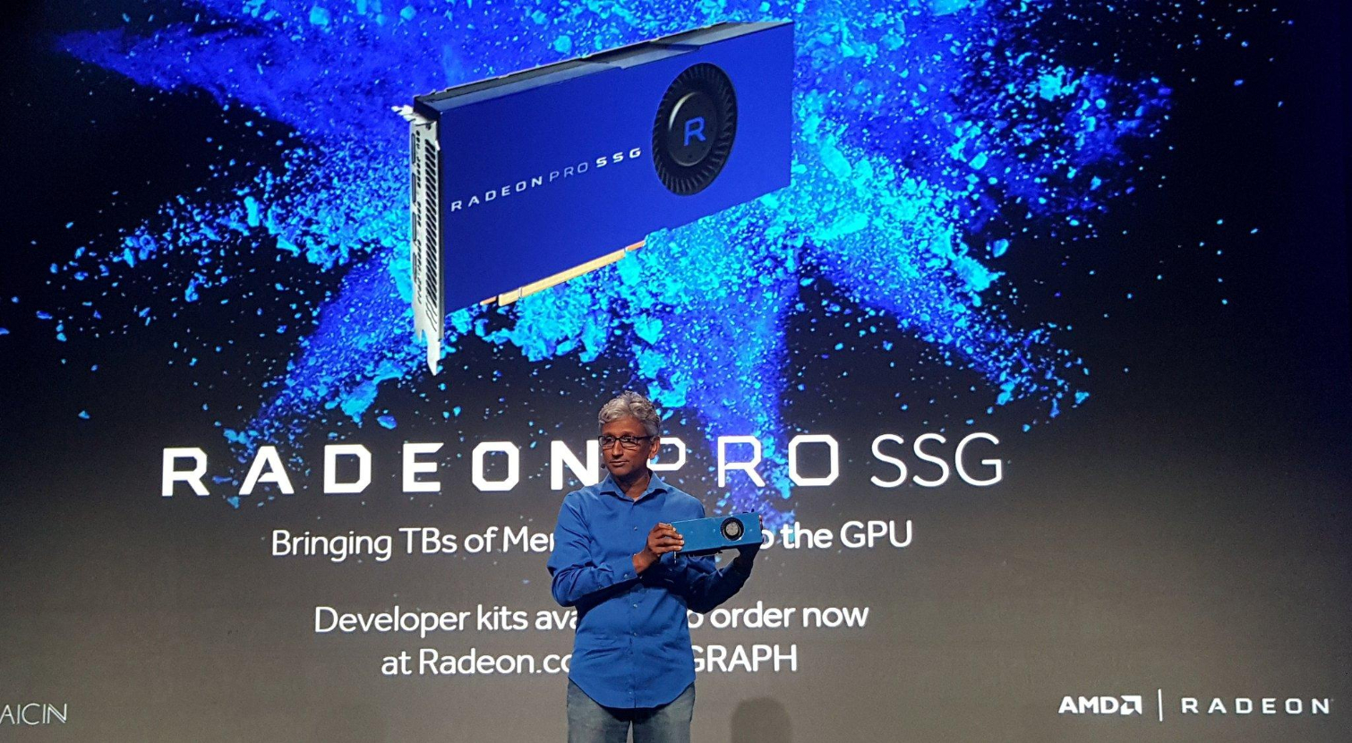
AMD's recent unveiling of its Radeon Pro SSG at SIGGRAPH created waves because the company announced that it had integrated M.2 SSDs on board its latest Fiji workstation GPU. While the move was unexpected, the possibilities are intriguing.
The company began a secret initiative in May 2013, code-named "Project Delta," with the goal of providing 1TB+ of non-volatile memory that is directly accessible to the GPU. Adding an on-board storage volume cuts through the various layers of hardware, software and OS interaction and provides a big increase in large data set performance.
The company presented an impressive demo that compared the performance of a normal workstation GPU with its new SSD-powered Radeon Pro SSG. The standard configuration was only able to provide 17 FPS with 8K video, while the SSG was able to scrub the 8K video in real time at 92 FPS. The quick demo and lack of further details have spawned incredible interest in the new architecture, so we followed up with AMD for more on the specifics on how the system works.
Article continues belowThe Mechanics
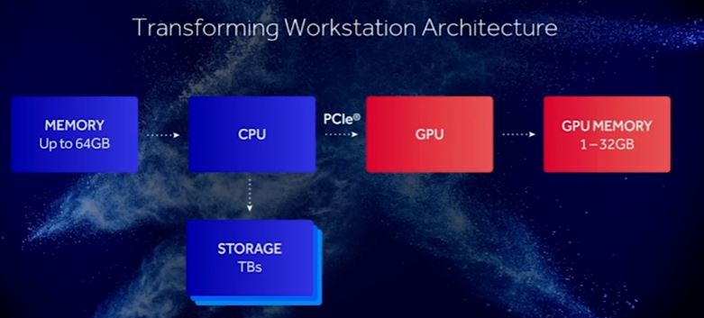
A standard system topology consists of a GPU with its on-board memory (usually somewhere between 1 - 32GB), separated from the storage pool and system memory by the PCIe bus. A GPU has to move data continuously between either the main system memory or the storage pool when it is processing a large data set that exceeds the size of the on-board memory. Transferring the data requires traversing both the PCIe bus and the CPU, which creates system overhead and increases latency.
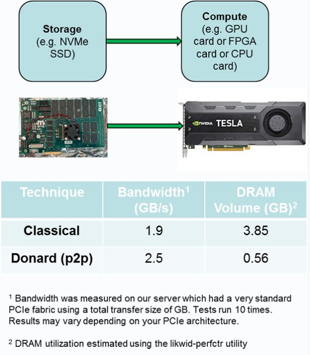
Moving data between storage and the GPU requires the CPU to stage the data in system DRAM, which consumes DRAM capacity and bandwidth, along with CPU cycles. There are techniques to reduce the overhead and additional latency that the extra steps incur, such as peer-to-peer (p2p) messaging techniques between NVMe SSDs and GPUs (see Project Donard). These techniques provide faster access to the adjacent memory/storage pools, but still require traversing the PCIe bus, which always incurs performance penalties. On a side note, Nvidia's NVLINK technology also uses a p2p technique to enhance communication performance between two GPUs, but it differs architecturally from p2p techniques that employ SSDs.
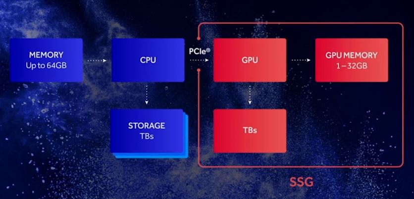
AMD's solution is simple from a hardware standpoint. The company connected two M.2 slots (PCIe 3.0 x4) directly to the GPU with a PEX8747 PCIe bridge chip, which creates a "private" PCIe bus and gives the GPU complete p2p control of the SSDs (and not the CPU/OS). AMD claims this reduces latency up to 10x and reduces PCIe bus contention.
Either the GPU can have its own private storage volume that is hidden from the OS, or it can share the SSD with the operating system, which adds several interesting possibilities for sharing the same data set with the CPU for additional processing. The current developer kit allows the operating system to see the storage pool, but AMD indicated that developers could use it as a private or shared pool in the future. AMD uses two 512GB Samsung 950 PRO SSDs in a RAID 0 configuration, which provides the bandwidth needed to use the storage as a 1TB extended frame buffer.
Get Tom's Hardware's best news and in-depth reviews, straight to your inbox.
An interesting side note: AMD currently employs HSA (Heterogeneous System Architecture) in its APUs. The HSA framework provides numerous benefits that allow the disparate components (CPU, GPU, memory) to function as one heterogeneous unit. One of HSA's most compelling features is its ability to allow the CPU and the GPU to simultaneously work on the same sections of the memory, which eliminates the need to shuffle data back and forth, as noted in our recent coverage.
HSA provides a pool of cache-coherent shared virtual memory that eliminates data transfers between components to reduce latency and boost performance. For instance, when a CPU completes a data processing task, the data may still require graphical processing. This requires the CPU to pass the data from its memory space to the GPU memory, after which the GPU then processes the data and returns it to the CPU. This complex process adds latency and incurs a performance penalty, but shared memory allows the GPU to access the same memory the CPU was utilizing, thus reducing and simplifying the software stack.
Theoretically, HSA would work well with a shared storage volume between the CPU and GPU, but AMD declined to answer if it is working on implementing core functions of the HSA framework with the Radeon Pro SSG at this time.
Where Is The Bottleneck?
AMD's demo consisted of a comparison of a high-performance system (+$10,000) with a normal RAID 0 pool created with two PCIe 3.0 x4 Samsung 512GB 950 PRO SSDs on the motherboard and a competing Radeon Pro SSG card with a similar on-board storage pool. The workstation provided 17 FPS during real-time 8K video editing with the RAID 0 storage array located on the motherboard, and the storage provided 848 MBps of throughput.
The SSG-powered system provided a stunning increase to 92 FPS during the same workload, and the onboard RAID 0 volume provided 4.59 GBps of throughput (it spiked over 4.6 GBps on several occasions). A single 950 PRO provides up to 2.5 GBps of sequential read throughput, so the results indicate that AMD is achieving near-linear RAID scaling. AMD specified that it achieved the results on early software and hardware, which implies that the company feels it can provide more performance as the platform matures.
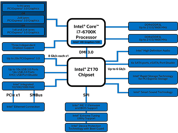
We were initially somewhat skeptical of the test results because the chipset bottlenecks most M.2 SSD RAID implementations. Data flows between the PCH and the CPU through the DMI connection, which is limited to a PCIe 2.0 x4 connection (or slower) on all pre-2015 systems, while modern systems employ the still-limited PCIe 3.0 x4 connection. A handful of motherboards sidestep the PCH/DMI by connecting a few M.2 PCIe lanes directly to the CPU, but the technique is not widespread, and we are not aware of any motherboards that use the technique with two M.2 SSDs.
The DMI limits the effective bandwidth of the on-board RAID 0, but there are options to use M.2 SSDs in a carrier card designed for the standard PCIe slot, or even a dedicated PCIe SSD placed into an adjacent PCIe slot. Both of these solutions would remove the DMI bottleneck, but AMD replied that its SSG implementation is actually faster than using a secondary PCIe SSD in a p2p connection scheme due to the increased latency and bus contention involved with communicating between the two devices. The company also indicated during the presentation that most workstations do not have free PCIe slots to add extra storage devices.
RAID 0 provides the ultimate in data performance, scaling and density, but it is also inherently unsafe to use with mission-critical data. While RAID 0 may be arguably safer with SSDs than with HDDs, it is still risky because a two-drive RAID doubles your exposure to possible component failure, and the risk increases with each additional SSD in the RAID array.
Businesses use the overwhelming majority of workstation GPUs, so the data has financial significance. Businesses do not take casual exposure to failures, and thus data loss, lightly. There are techniques to increase the resilience of the storage pool, such as using RAID 5 or 6, but these require more than two SSDs, which may be a limiting factor for the space-constrained GPU. Complex types of RAID require more processing power, which is hardly a problem when the storage is bolted onto a massive parallel computing device, but they also slow down performance, increase latency, and reduce the amount of usable storage capacity.
So, Is It Storage, Or Memory?
The industry is beginning to enable the use of persistent memory, such as 3D XPoint and NAND, as an additional layer in the overall memory pool. These techniques involve using the non-volatile memory (in this case NAND) as an adjunct to RAM by mapping it as memory in a flat memory model. This means that the system will only see one large pool of RAM even though large portions, and in some cases even the majority, of the capacity will consist of other mediums (NAND, 3D XPoint).
Of course, NAND and 3D XPoint are slower than GDDR5, so there is a performance impact if the system needs to access the data the GPU holds in NAND, but the benefit of exponentially increasing the addressable memory far outweighs the drawbacks.
Using non-volatile memory as RAM is a hot topic thanks to the impending arrival of Intel/Micron's 3D XPoint. Several initiatives are underway in the Linux community (pmem.io is a good example) and in Windows (Microsoft will support it in Server 2016) to support non-volatile memory working in tandem with system memory, so the underpinnings of the technology are well underway.
Most implementations are being developed to use non-volatile memory (storage-class memory) on the RAM bus, such as with NVDIMMs, UltraDIMMs and Memory1, but the PMC-Sierra Flashtec NVRAM drive (review here) is a great example of using a memory-mapped device on the PCIe bus with the NVMe protocol. ECC RAM for professional applications can cost as much as $8/GB, while raw NAND can be purchased for $0.30/GB, so using NAND as memory lowers cost and increases density, as evidenced by the 256GB Diablo Memory1 NAND DIMMS (pictured).
AMD indicated that it is not using the NAND pool as a memory-mapped space currently, but it can do so, and it is a logical progression of the technology. The company also commented that some developers are requesting a flat memory model. Even though the company provides the entire pool as storage, in the future it can partition a portion of the pool, or all of it, to operate as memory, which will open the door to many more architectural possibilities.
The Radeon Pro SSG is making its debut with 1TB of SSD storage, but this isn't an absolute; the company indicated that the capacity of currently available M.2 SSDs is the limiting factor, not its ability to manage a high-capacity pool. There is a clear path forward as the industry shifts to denser 3D NAND, which some project can offer up to 10 TB of storage per M.2 SSD.
Even with copious amounts of on-board storage, there will always be workloads that require more, so deciding what to cache in the NAND-based storage on board the card becomes a challenge. If the GPU requests data that is absent from the on-board storage pool, it will require a latency-inducing grasp for data held on the normal storage volume, which triggers the long trip across the system PCIe bus and CPU. These requests are referred to as cache misses, and they incur significant performance penalties, and in some cases can result in severe stuttering or hitching.
Assuring that the correct data is in the right place at the right time will become a big focus for developers, and the same principles apply if the system is using NAND as either storage or memory, though it becomes more complex and resource intensive when the GPU uses it as memory. Much like other caching/tiering implementations found in the storage world, there are algorithms that can automatically detect the most commonly accessed data (hot data) and preemptively move it into the on-board RAID 0 pool to minimize cache misses. In many cases, deciding which cold data to evict (de-stage) from the cache is just as important as identifying hot data, because it maximizes the impact of the usable capacity.
Cache misses are worrisome, and some existing read-ahead techniques grab all the data surrounding a cache miss (the contiguous data) and simply pull it into the cache to minimize the chance of successive misses. However, there are newer and more refined machine-learning-like algorithms that can detect trends and predictively place data (prefetch) in the cache based upon usage history. Machine learning algorithms would likely be the best approach, as the storage is adjacent to the GPU, which is one of the most commonly used platforms for the task. Current memory/NAND merging technologies also allow users to define QoS (Quality of Service) parameters that will prioritize data traffic based upon specialized use cases.
AMD is also providing hooks for developers so they can selectively pin data directly into the storage pool. The leading edge implementations will require dedicated coding to extract the maximum possibilities, but there are techniques that can abstract the complexity of the underlying tiered/cached architecture away from the developers, and as the ecosystem evolves we expect those tactics to become commonplace. These refined methods will remove some of the challenges (and cost) associated with custom coding, thus increasing the number of workloads that can use the technology (at least easily).
But Doesn't Flash Die?
One of the best aspects of the current SSG, at least from AMD's standpoint, is that modern SSDs are self-contained units. The SSD manages all of the internal processes, so it handles garbage collection, wear leveling and other tasks without intervention. AMD indicated that NVMe and the M.2 specification provide an existing and mature platform, and using existing technology speeds the development process. Future types of memory, such as 3D XPoint, will use the existing protocols and specifications, so it also provides a clear evolutionary path with other mediums that use the plug-and-play standards.
AMD indicated that it is taking numerous steps to leverage its control of the GPU to increase the endurance and performance of the SSDs, which have a finite lifespan and limited performance, but it isn't revealing specifics at this time. A single 512 GB 950 PRO features a 400 TBW (Terabytes Written) rating, and placing the SSDs into RAID 0 spreads the workload between the two SSDs, which effectively doubles endurance to 800 TBW. This means the RAID array can absorb nearly a petabyte of random write data before the SSDs expire. Much of the data will likely be read centric, which doesn't reduce endurance (by a large amount, at least), and the GPU can further optimize endurance by absorbing all write traffic in the GDDR5, which has unlimited endurance, and only flushing it to the NAND if the changes are permanent.
AMD can increase both endurance and performance simply by using sequential data. SSD vendors spec the endurance of a drive based upon harsh random write workloads, which wear the NAND quickly due to the read, write, modify process that is required when the SSD writes random data (in steady state). However, sequential workloads are much less taxing on NAND-based storage, which leads to an increase in endurance. For instance, Micron lists the endurance of its 3.2TB 9100 NVMe SSD at 3.28 PB with random data, but it nearly triples to 9.6PB with sequential traffic. If developers code the GDDR5 to absorb all incoming write traffic, it can flush any permanent data changes to the NAND sequentially at its leisure, thus extending the NAND's lifespan.
The same endurance-boosting principles apply to nearly all flash storage mediums, so it is likely that AMD and developers will use similar techniques. The Radeon SSG also employs standard M.2 SSDs, which means that users should be able to replace an SSD if it exceeds its endurance threshold. It is also easy to envision that AMD will enable some sort of SMART monitoring, which includes thermal and endurance data.
Sequential data is also faster than random data access, so assuring that the GPU writes all data to, and retrieves it from, the RAID 0 array sequentially will assure high performance and extremely low latency. It is also easy to imagine the company using custom daughter cards with embedded controllers to increase density and performance, but it did not comment on its future plans.
What About Heat And Power?
SSDs are sensitive to heat, but M.2 SSDs are much more sensitive than other variants because they do not have an embedded heatsink. The small SSDs throttle under heavy load or in high-heat conditions, but often the throttling is dynamic and hard to detect. In either case, placing an M.2 SSD inside the space heater that is a modern GPU raises concerns.
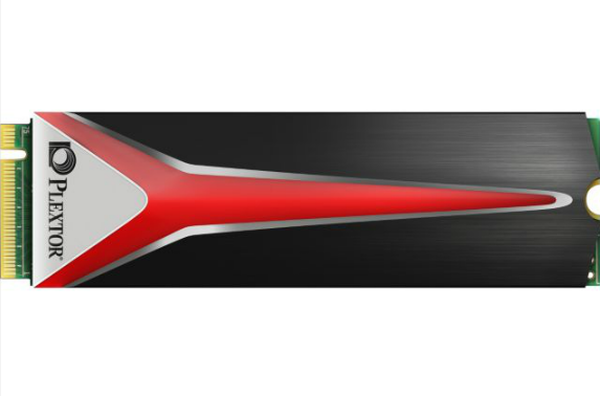
The M.2 specification does not include any standardized way to affix heatsinks, but some emerging M.2 SSDs, such as the Plextor M8Pe, employ custom designs. There are also several carrier cards designed to mate with M.2 SSDs to keep them cool, and even watercooling adapters.
AMD indicated that it isn't experiencing SSD throttling within its specifications and TDP (although it would not disclose the actual TDP), but it also indicated that its active cooling system would be used in conjunction with the SSDs to keep them cool. In other words, the GPU heatsink will be affixed to the M.2 SSDs. Most SSDs begin to throttle around 85°C, and the large active cooling solutions should be able to keep the SSD under that temperature threshold during heavy use.
Samsung spec’d its 950 PRO at 5.1W, but the minor power draw is hardly a concern for a workstation GPU. Modern GPUs are reaching the limits of power consumption due to their on-board memory, so if the GPU uses NAND as memory in the future, it will actually help to alleviate excessive power consumption concerns, thus potentially allowing for more addressable memory.
Real-World Use Cases
The list of potential use cases where AMD's SSG could provide substantial benefit is almost limitless: genome sequencing, media and entertainment (M&E), medical imaging, and oil and gas exploration, just to name a few. Oil and gas exploration, for instance, uses multiple large data sets simultaneously. Expanding memory by orders of magnitude can widen the geographical window of observation from a few miles to an entire region, increasing productivity and enhancing the ability to identify trends.
Some medical imaging applications can image body processes, like a beating heart, in real time, providing physicians with an unprecedented view compared to a static 2D image. Real-time viewing increases the physician's ability to make correct a diagnosis, but the massive amount of data currently limits these views to a few seconds, while the expanded storage on board the Radeon SSG could potentially expand that to minutes.
Administrators are using GPUs for more diverse use cases in the data center, such as machine learning and boosting database performance, and having a much larger working data set can expand the reach and performance of these types of applications as well.
The Line Between Storage And Memory Blurs
The operating system becomes the barrier with many file transfer operations, so moving data directly onto the GPU gives AMD an easy way to boost performance for large data sets. Reducing traffic over the PCIe bus for file transfers during real-time tasks will reduce bus contention, which has other benefits as well.
The current implementation merely uses the SSD as a storage volume for frequently-accessed data, but as the technology progresses to a memory-mapped model the performance advances should become even more pronounced. Storage aficionados have long decried how we use NAND because even after nearly five years of semi-mainstream use we still aren't using it to its full potential. However, as the industry develops innovative ways to fuse it into the memory hierarchy we are coming closer to realizing its true capabilities. Some of the greatest computing advances have come from moving data closer to the CPU by migrating NAND to the PCIe or memory bus, and the Radeon Pro SSG takes a similar approach by moving the data closer to the GPU compute resource.
NAND is much cheaper than DRAM, and it also consumes a mere fraction of the power required for GDDR5, which also limits the maximum amount of memory that the vendors can design into the card. The combination of lower cost and power consumption is a win, and we expect this technique to gain traction and evolve quickly.
AMD is selling developer kits that will become available in 2017, and considering that these are the leading-edge products, it will likely be awhile before this bleeds over to the enthusiast market, but it will. Most game data, especially for 1920x1080 resolutions, fits nicely within the boundaries of GDDR5 capacity. However, as gaming moves to more demanding 4K and 8K resolutions (particularly multi-monitor) the need for more memory will becoming pressing enough to move the technology to the mainstream.
The implications for VR, which, almost by definition, uses massive data sets, are incredible. The timeline indicates that NAND-infused GPUs will remain on the horizon for some time, and we may already be at 4 TB per M.2 SSD by the time enthusiast-class products come to market, which is exciting. One would almost predict that the first enthusiast-class GPUS with on-board SSDs will be aimed specifically at VR workloads.
One of the great things about the Radeon Pro SSG is that it denotes that AMD is clearly thinking futuristically and enabling the hardware components that power a flat memory model. The company is also obviously laying the foundation for larger, faster and more endurant persistent memory technologies, such as 3D XPoint, in the future.
MORE: Best SSDs
MORE: Best Memory
MORE: Best Graphics Cards

Paul Alcorn is the Editor-in-Chief for Tom's Hardware US. He also writes news and reviews on CPUs, storage, and enterprise hardware.
-
Xajel The Idea is impressive, although I don't see any use for it in our consumer applications..Reply
I think having the PCIe lanes in the GPU it self ( in addition the x16 lanes to connect to the CPU/chipset ), though I don't know how much better this will be compared to using a bridge chip, specially with the complexity of having a host PCIe in the GPU -
danlw Genome sequencing? Geological mapping? Real-time heart imagery?Reply
This reminds me of one of those faux 1960s motivational posters...
VIDEO GAMES! (Why waste good technology on science and medicine?) -
babernet_1 Imagine having this on a gaming GPU. You could load all the levels and textures and all on the internal SSD so your game would never pause between levels or new areas.Reply -
BoredSysAdmin The whole TWO Paragraphs (in Bottleneck section) are dedicated to how RAID 0 sucks and biz uses raid 5/6, while these are not-untrue - they also very much irrelevant to the point. The storage on GPU is meant to be temporary by definition so in this context - raid 0 is fine choice.Reply
Not to mention Samsung Pro are one of most reliable SSDs on the market today and chances of sudden death are practically none-existent.
Also the point of bottleneck should be made more clearly - very limited implementation of DMI on consumer CPU sucks and even use of PCIe SSD doesn't solve issue of latency. -
none12345 I also think the rant on raid 0 is misplaced. With SSDs its largely irrelevant.Reply
Lets for a minute compare a SSD with 4 flash chips and 256GB vs an SSD with 8 flash chips and 512 GB of storage. There is very little difference between having 2 of those 256gbs in one enclosure in raid 0 vs having the single 8 chips drive in that enclosure. Sure there are 2 controller chips in taht instance, so another controller chip to die, but really there is no practical increased risk of failure.
Having more bandwidth by using 2 controller chips is definitely the right choice in this instance. You could argue for more then 2 if you needed more bandwidth. If one controller chip could cut it, you don't need 2 tho. -
Paul Alcorn Reply18407386 said:I also think the rant on raid 0 is misplaced. With SSDs its largely irrelevant.
Lets for a minute compare a SSD with 4 flash chips and 256GB vs an SSD with 8 flash chips and 512 GB of storage. There is very little difference between having 2 of those 256gbs in one enclosure in raid 0 vs having the single 8 chips drive in that enclosure. Sure there are 2 controller chips in taht instance, so another controller chip to die, but really there is no practical increased risk of failure.
Having more bandwidth by using 2 controller chips is definitely the right choice in this instance. You could argue for more then 2 if you needed more bandwidth. If one controller chip could cut it, you don't need 2 tho.
It is true that the data held in the GPU memory space is transitory in nature, but there are caveats to how it is used. The memory can be used as a storage volume, so data that needs persisted (stored) will be located in the RAID 0, so losing that data to a RAID 0 failure does place the user in a position to lose data. Also, if one were working with the NAND as memory and the RAID failed, all of that data, and thus work, would be lost. Not to mention the disadvantage of downtime, RMA, etc. The time expended to right the situation, even if the data itself was temporary, equates directly to lost money.
RAID 0 is inherently risky, and it doesn't matter what you use as a storage medium. There is no single storage device that has a zero chance of failure. ALL storage devices fail, given enough time.
Yes, as noted, SSDs are arguably safer, but the nature of SSD failures usually involves surface mount components on the PCB, and not the controller or NAND, so you are exposing yourself to more components, and thus failure. There are also firmware issues (freezing, locking) that are doubled when you have two separate SSDs. The M.2 sockets are also another possible point of failure, and that is doubled. As with any design, when you multiply the number of components you multiply the possible points of failure.
-
none12345 I think the raid argument is completely moot.Reply
There is absolutely nothing stopping someone from making a M.2 ssd that has 2 ssds in raid 1 instead of 2 in raid 0. Or 3 in raid 5, or 100 in raid 6, or whatever else configuration of controllers and flash packages they want. The card never has to see any of that nor care about how the data is stored after the connector. Let the customer decide what they want to plug into that M.2, its a trivial matter. -
Paul Alcorn Reply18410857 said:I think the raid argument is completely moot.
There is absolutely nothing stopping someone from making a M.2 ssd that has 2 ssds in raid 1 instead of 2 in raid 0. Or 3 in raid 5, or 100 in raid 6, or whatever else configuration of controllers and flash packages they want. The card never has to see any of that nor care about how the data is stored after the connector. Let the customer decide what they want to plug into that M.2, its a trivial matter.
I agree, there are other options, as mentioned in the article.
-
fixxxer113 Reply18405115 said:Imagine having this on a gaming GPU. You could load all the levels and textures and all on the internal SSD so your game would never pause between levels or new areas.
I think that's the end goal. Storage is slowly moving towards having one big pool that's fast enough to be used for anything (data storage, RAM, VRAM etc.). It would also simplify the architecture of a PC, since you wouldn't need all kinds of different slots and maybe make graphics cards smaller, if their VRAM was no longer on the PCB but part of one big chunk of memory/storage connected to the motherboard.
If anything, the evolution of hardware until now has shown that it's a matter of time before we get to a point where we have ridiculous amounts of extremely fast storage with a low cost.
