Arm Details Neoverse V1 and N2 Platforms, New Mesh Design
The ARMy lines up to take on x86
Yesterday marked the 36th anniversary of the first power-on of an Arm processor. Today, the company announced the deep-dive details of its Neoverse V1 and N2 platforms that will power the future of its data center processor designs and span up to a whopping 192 cores and 350W TDP.
Naturally, all of this becomes much more interesting given Nvidia's pending $40 billion Arm acquisition, but the company didn't share further details during our briefings. Instead, we were given a deep dive look at the technology roadmap that Nvidia CEO Jensen Huang says makes the company such an enticing target.
Arm claims its new, more focused Neoverse platforms come with impressive performance and efficiency gains. The Neoverse V1 platform is the first Arm core to support Scalable Vector Extensions (SVE), bringing up to 50% more performance for HPC and ML workloads. Additionally, the company says that its Neoverse N2 platform, its first IP to support newly-announced Arm v9 extensions like SVE2 and Memory Tagging, delivers up to 40% more performance in diverse workloads.
Additionally, the company shared further details about its Neoverse Coherent Mesh Network (CMN-700) that will tie together the latest V1 and N2 designs with intelligent high-bandwidth low-latency interfaces to other platform additives, such as DDR, HBM, and various accelerator technologies, using a combination of industry-standard protocols, like CCIX, CXL, and PCIe. This new mesh design serves as the backbone for the next generation of Arm processors based on both single-die and multi-chip designs.
If Arm's performance projections pan out, the Neoverse V1 and N2 platforms could provide the company with a much faster rate of adoption in multiple applications spanning the data center to the edge, thus putting even more pressure on industry x86 stalwarts Intel and AMD. Especially considering the full-featured connectivity options available for both single- and multi-die designs. Let's start with the Arm Neoverse roadmap and objectives, then dive into the details of the new chip IP.
Arm Neoverse Platform Roadmap
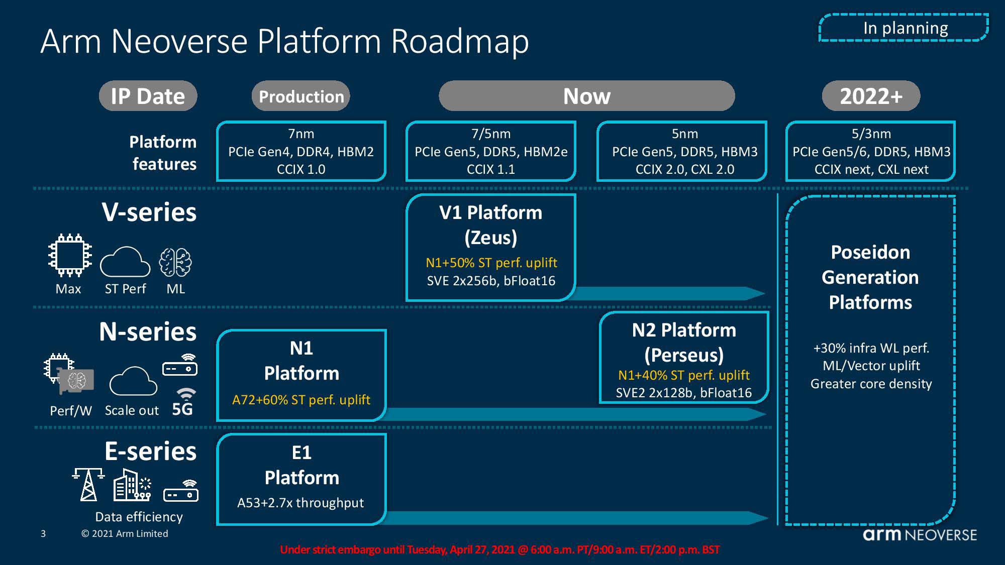
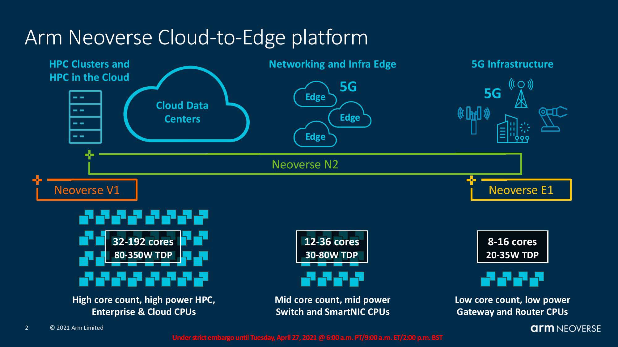
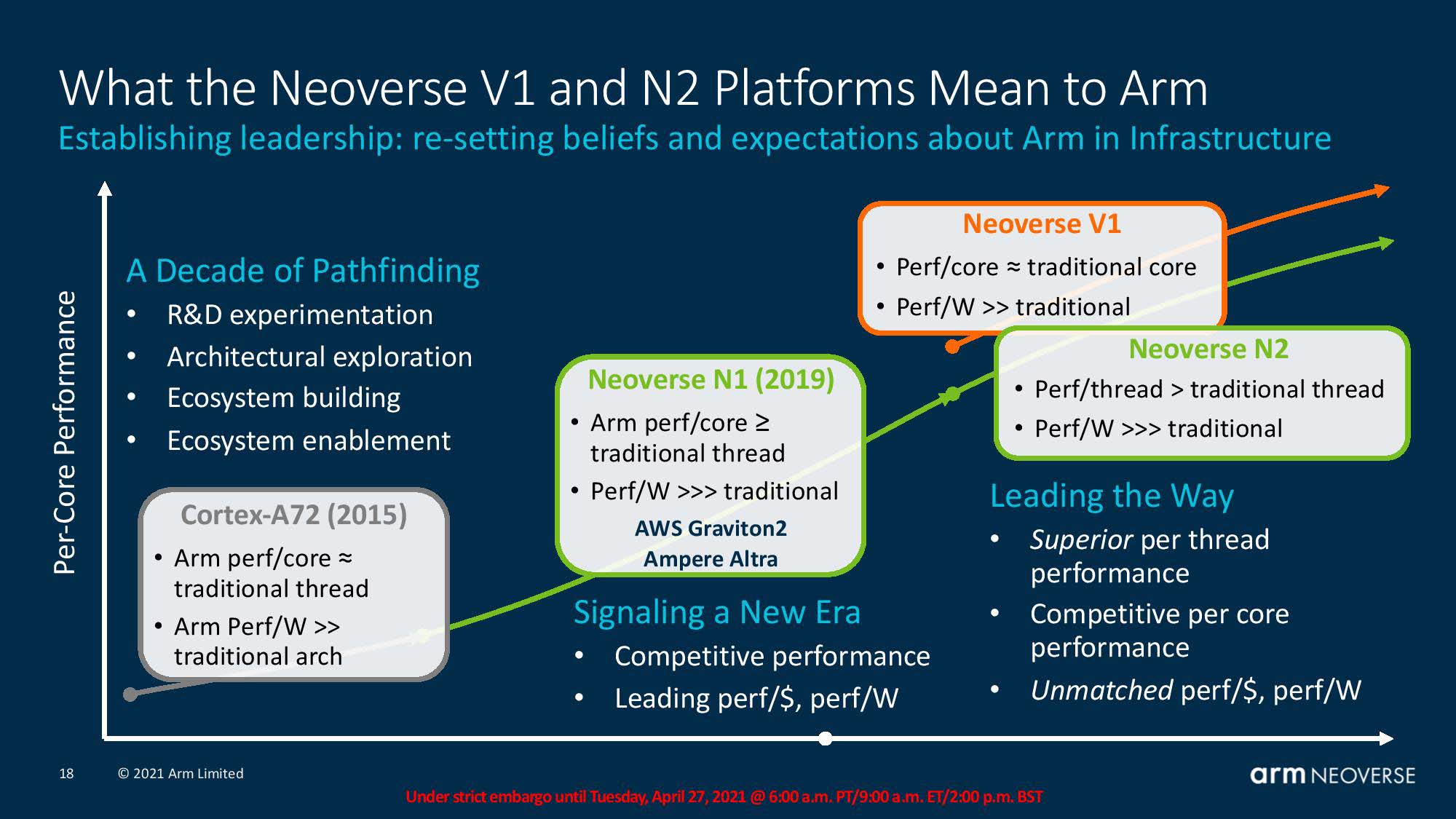
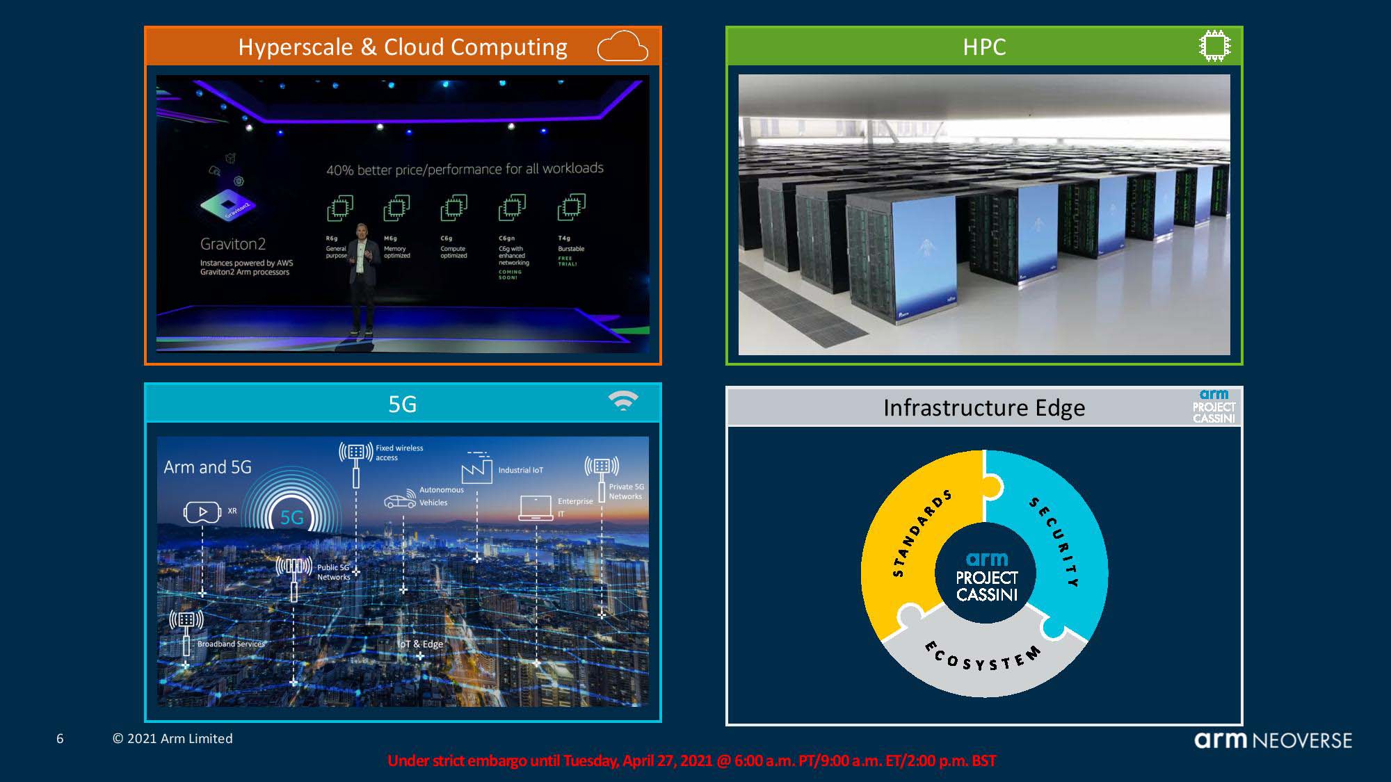
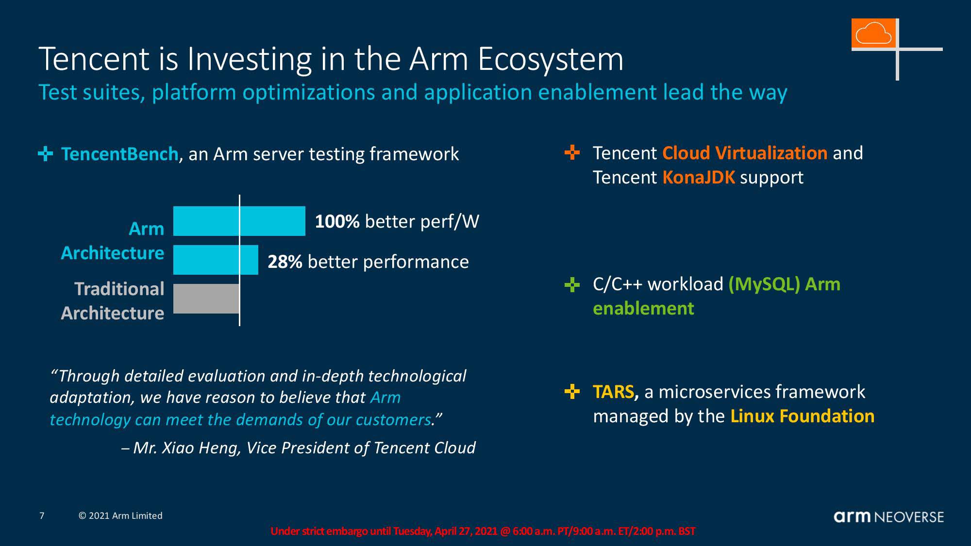
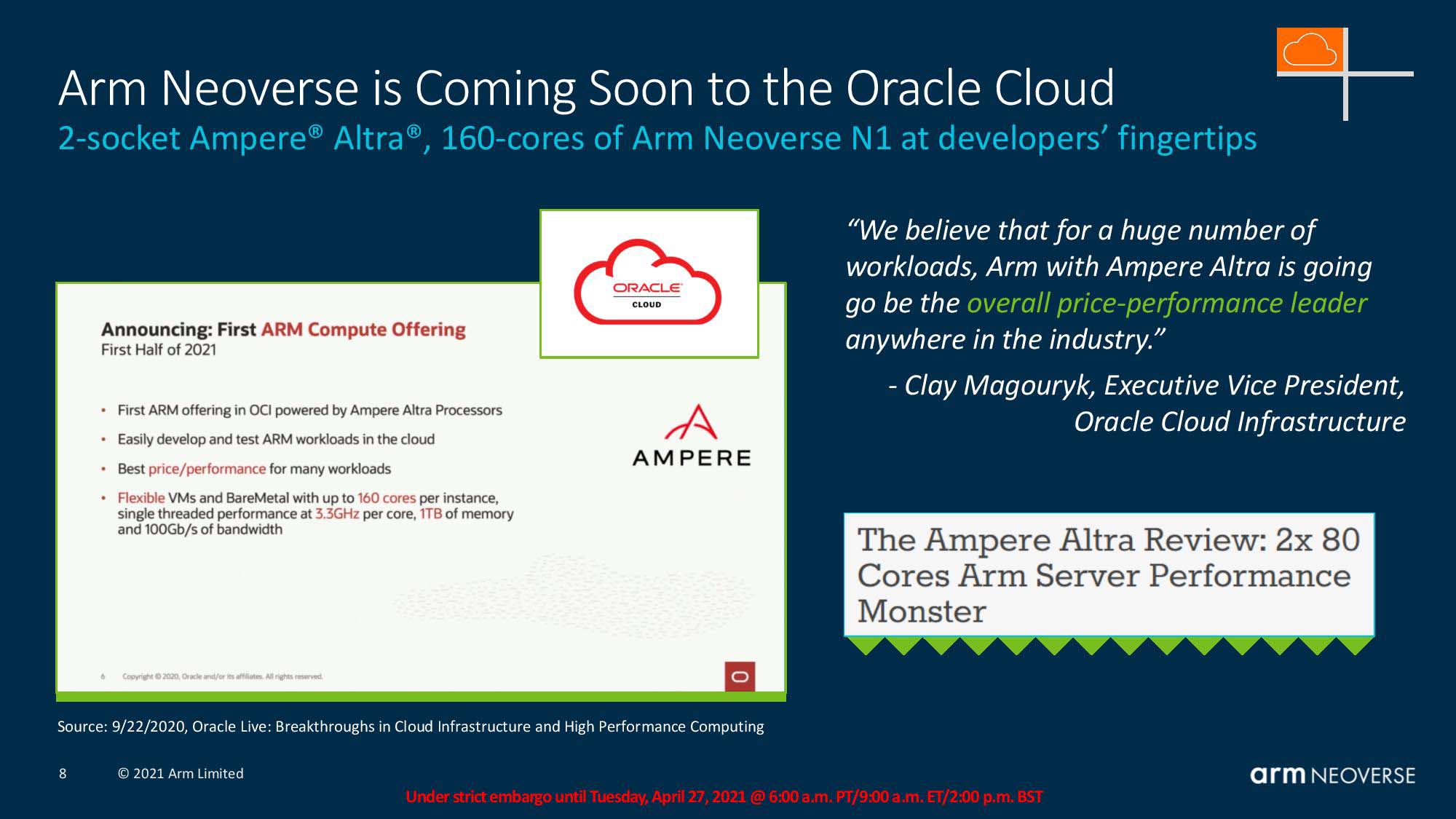
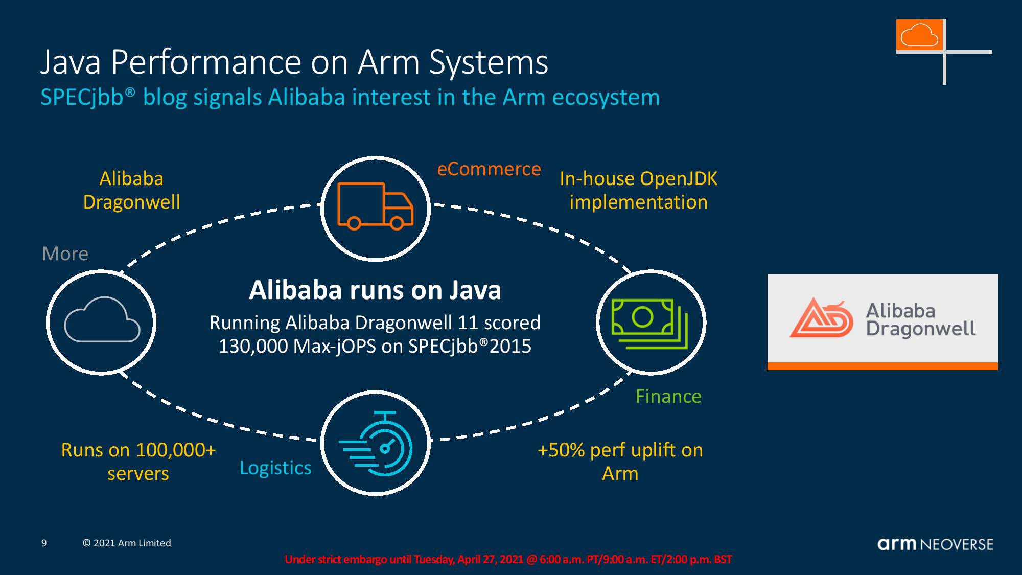
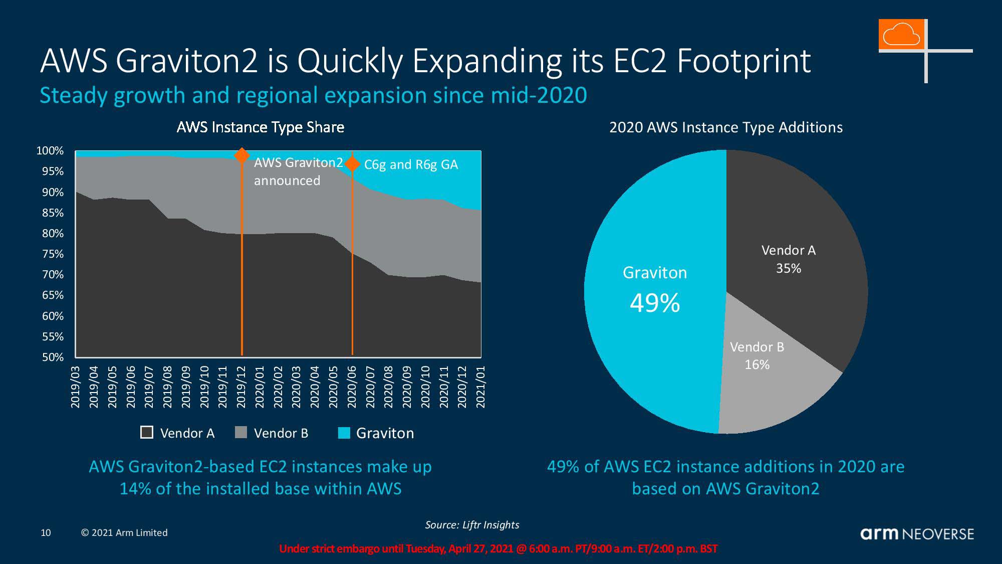

Arm's roadmap remains unchanged from the version it shared last year, but it does help map out the steady cadence of improvements we'll see over the next few years.
Arm's server ambitions took flight with the A-72 in 2015, which was equivalent to the performance and performance-per-watt of a traditional thread on a standard competing server architecture.
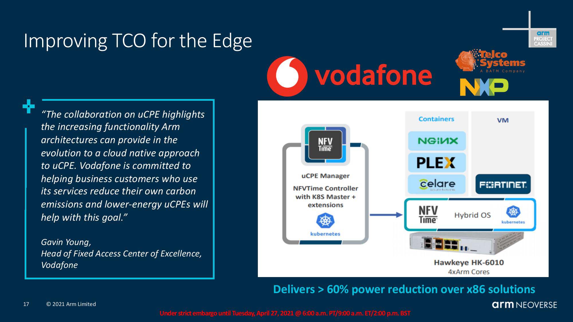
Arm says its current-gen Neoverse N1 cores, which powers AWS Graviton 2 chips and Ampere's Altra, equals or exceeds a 'traditional' (read: x86) SMT thread. Additionally, Arm says that, given N1's energy efficiency, one N1 core can replace three x86 threads but use the same amount of power, providing an overall 40% better price-vs-performance ratio. Arm chalks much of this design's success up to the Coherent Mesh Network 600 (CMN-600) that enables linear performance scaling as core counts increase.
Arm has revised both its core architecture and the mesh for the new Neoverse V1 and N2 platforms that we'll cover today. Now they support up to 192 cores and 350W TDPs. Arm says the N2 core will take the uncontested lead over an SMT thread on competing chips and offers superior performance-per-watt.
Additionally, the company says that the Neoverse V1 core will offer the same performance as competing cores, marking the first time the company has achieved parity with two threads running on an SMT-equipped core. Both chips utilize Arm's new CMN-700 mesh that enables either single-die or multi-chip solutions, offering customers plenty of options, particularly when deployed with accelerators.
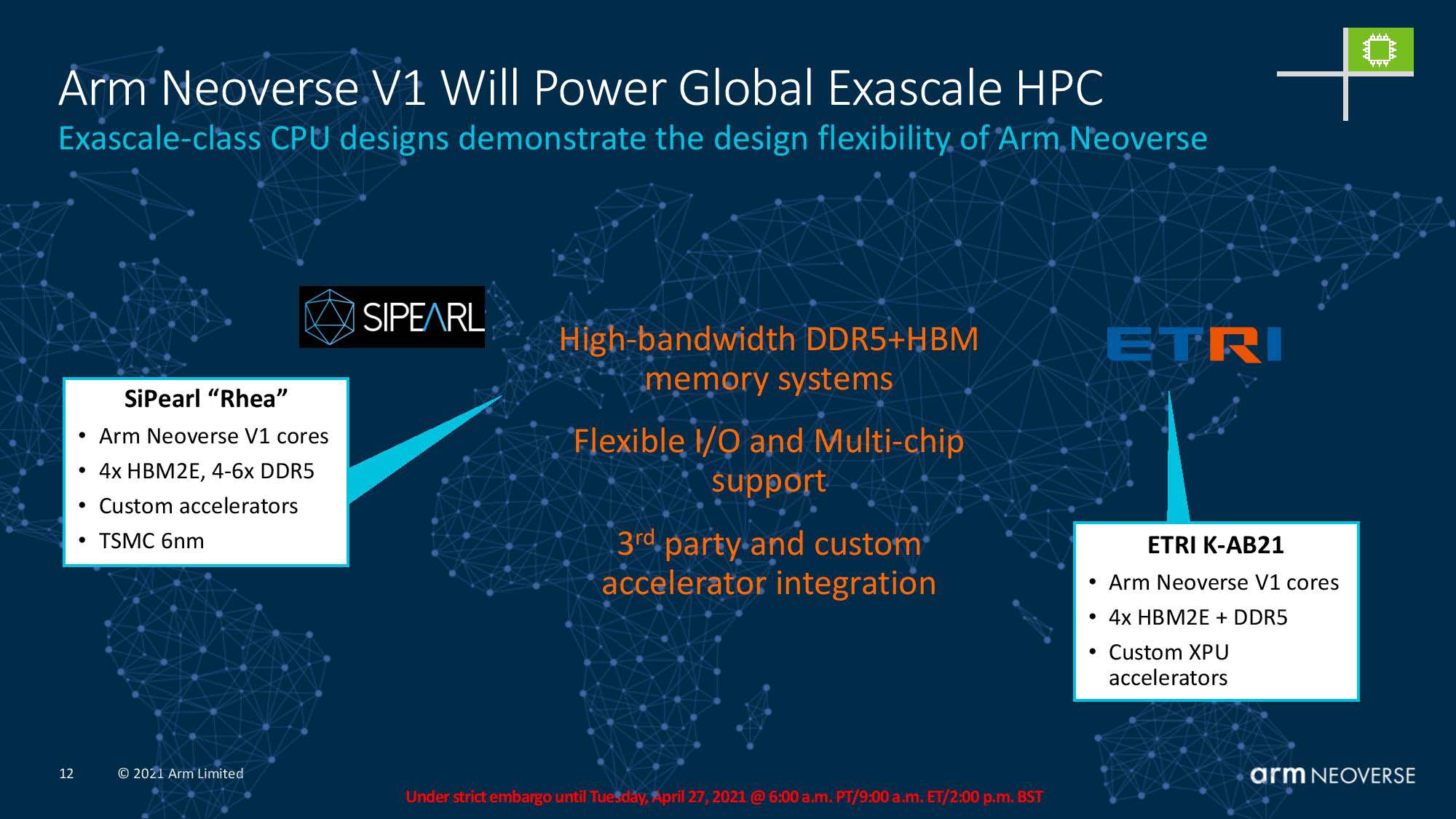
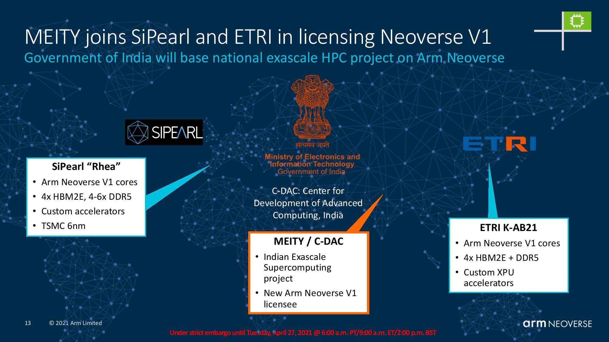
Ts one would expect, Arm's Neoverse N2 and V1 target hyperscale and cloud, HPC, 5G, and the infrastructure edge markets. Customers include Tencent, oracle Cloud with Ampere, Alibaba, AWS with Graviton 2 (which is available in 70 out of 77 AWS regions). Arm also has two exascale-class supercomputer deployments planned with Neoverse V1 chips: SiPearl "Rhea" and the ETRI K-AB21.
Overall, ARM claims that its Neoverse N2 and V1 platforms will offer best-in-class compute, performance-per-watt, and scalability over competing x86 server designs.
Get Tom's Hardware's best news and in-depth reviews, straight to your inbox.
Arm Neoverse V1 Platform 'Zeus'
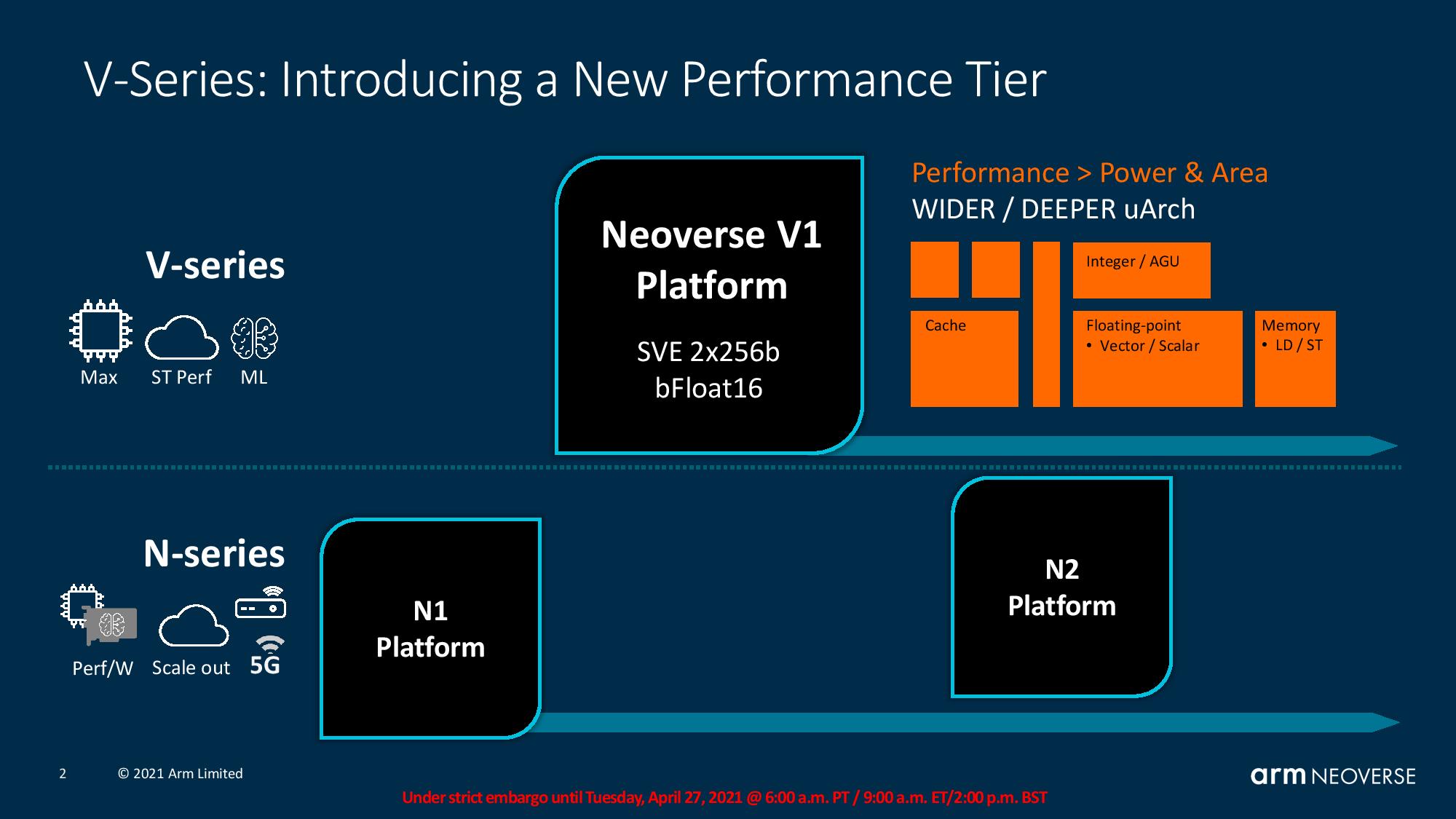
Arm's existing Neoverse N1 platform scales from the cloud to the edge, encompassing everything from high-end servers to power-constrained edge devices. The next-gen Neoverse N2 platform preserves that scalability across a spate of usages. In contrast, Arm designed the Neoverse V1 'Zeus' platform specifically to introduce a new performance tier as it looks to more fully penetrate HPC and machine learning (ML) applications.
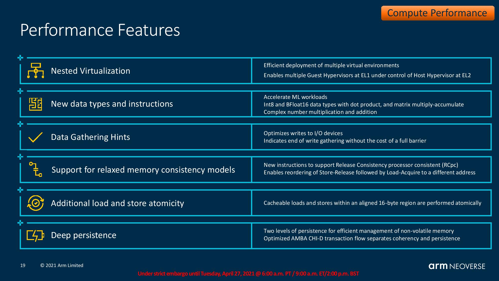
The V1 platform comes with a wider and deeper architecture that supports Scalable Vector Extensions (SVE), a type of SIMD instruction. The V1's SVE implementation runs across two lanes with a 256b vector width (2x256b), and the chip also supports the bFloat16 data type to provide enhanced SIMD parallelism.
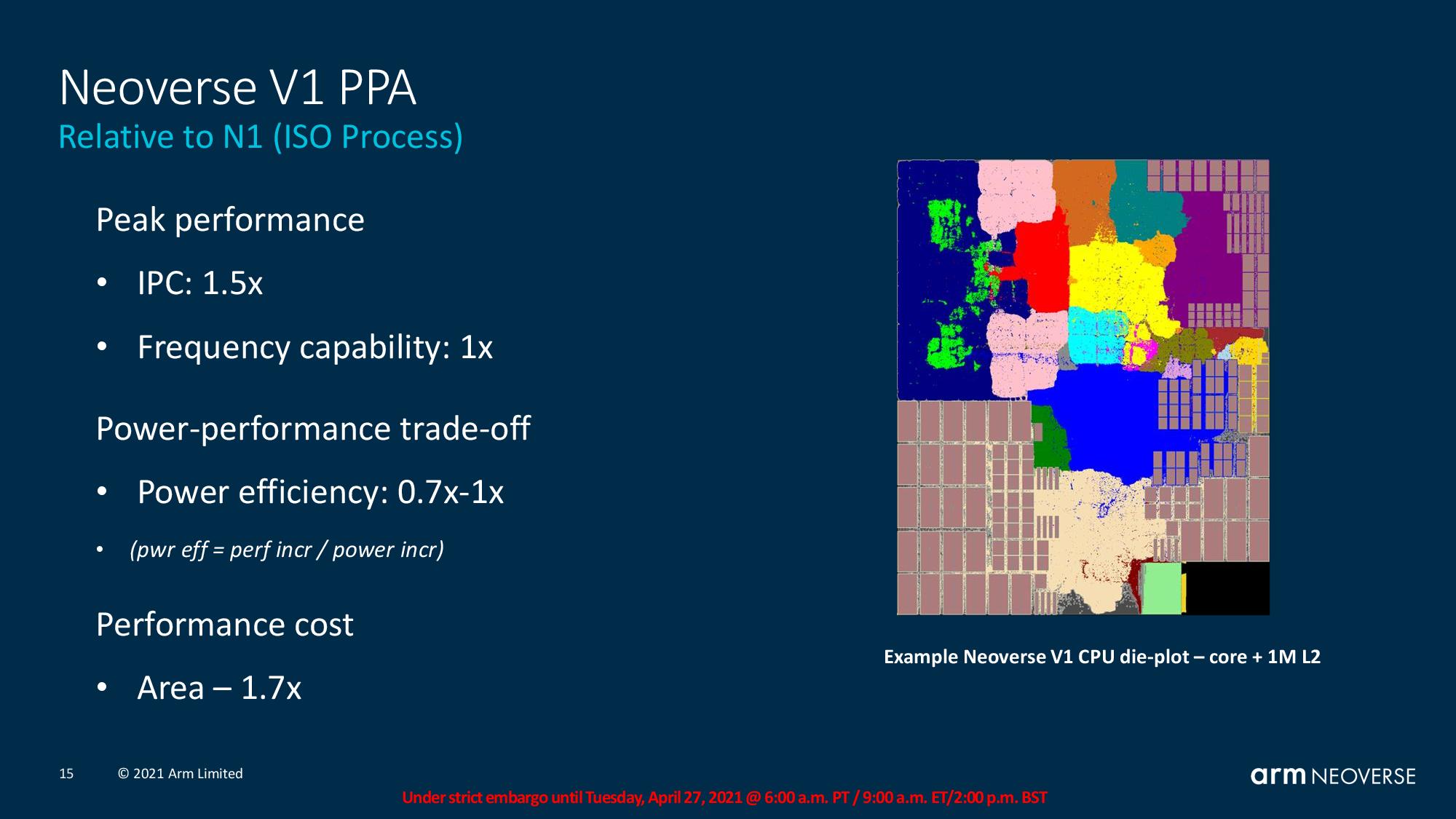
With the same (ISO) process, Arm claims up to 1.5x IPC increase over the previous-gen N1 and a 70% to 100% improvement to power efficiency (varies by workload). Given the same L1 and L2 cache sizes, the V1 core is 70% larger than the N1 core.
The larger core makes sense, as the V-series is optimized for maximum performance at the cost of both power and area, while the N2 platform steps in as the design that's optimized for power-per-watt and performance-per-area.
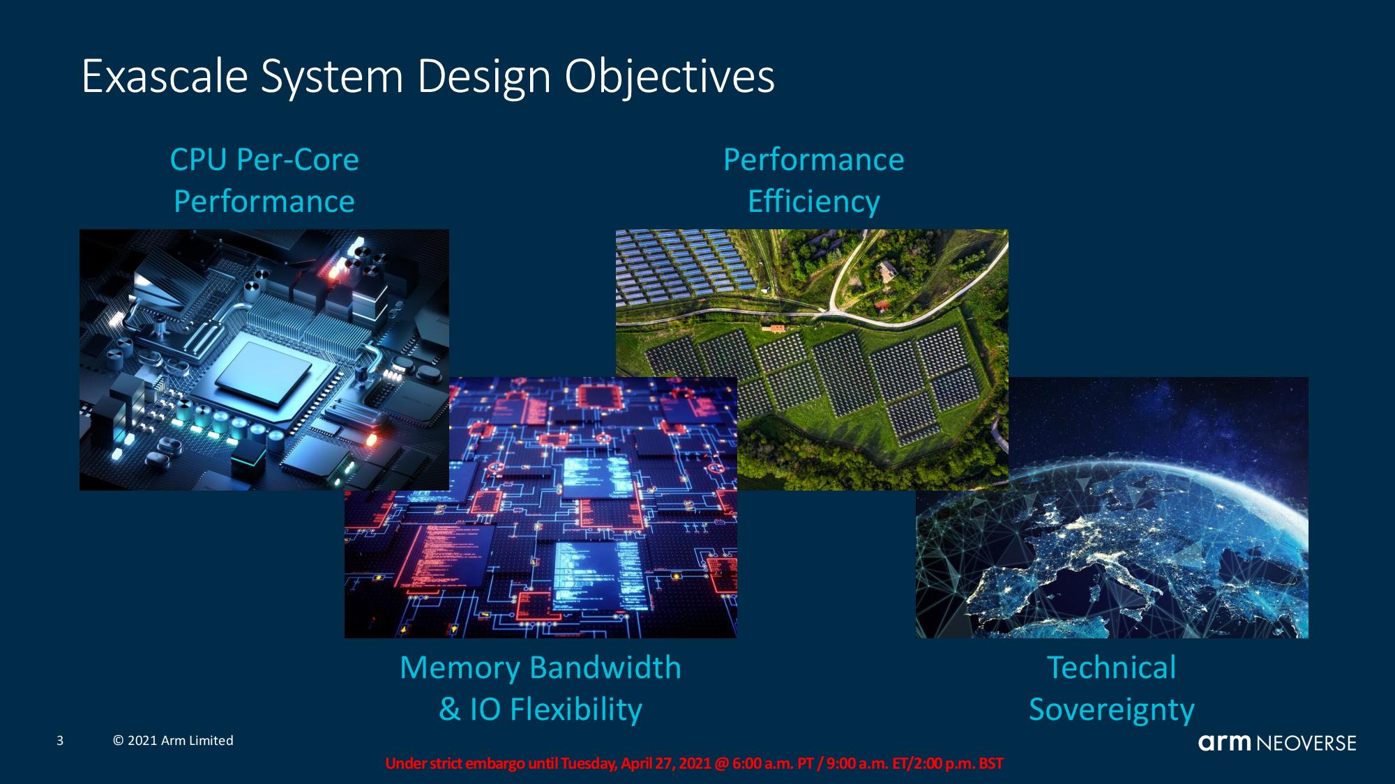
Per-core performance is the primary objective for the V1, as it helps to minimize the performance penalties for GPUs and accelerators that often end up waiting on thread-bound workloads, not to mention to minimize software licensing costs.
Arm also tuned the design to provide exceptional memory bandwidth, which impacts performance scalability, and next-gen interfaces, like PCIe 5.0 and CXL, provide I/O flexibility (much more on that in the mesh section). The company also focused on performance efficiency (a balance of power and performance).
Finally, Arm lists technical sovereignty as a key focus point. This means that Arm customers can own their own supply chain and build their entire SoC in-country, which has become increasingly important for key applications (particularly defense) among heightened global trade tensions.
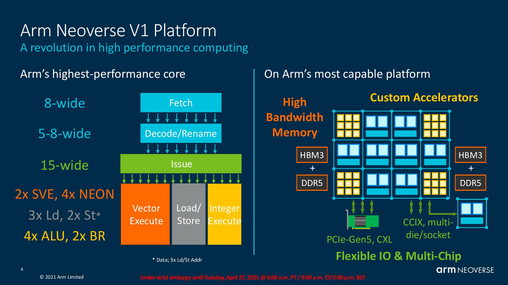
The Neoverse V1 represents Arm's highest-performance core yet, and much of that comes through a 'wider' design ethos. The front end has an 8-wide fetch, 5-8 wide decode/rename unit, and a 15-wide issue into the back end of the pipeline (the execution units).
As you can see on the right, the chip supports HBM, DDR5, and custom accelerators. It can also scale out to multi-die and multi-socket designs. The flexible I/O options include the PCIe 5 interface and CCIX and CXL interconnects. We'll cover the Arm's mesh interconnect design a bit later in the article.
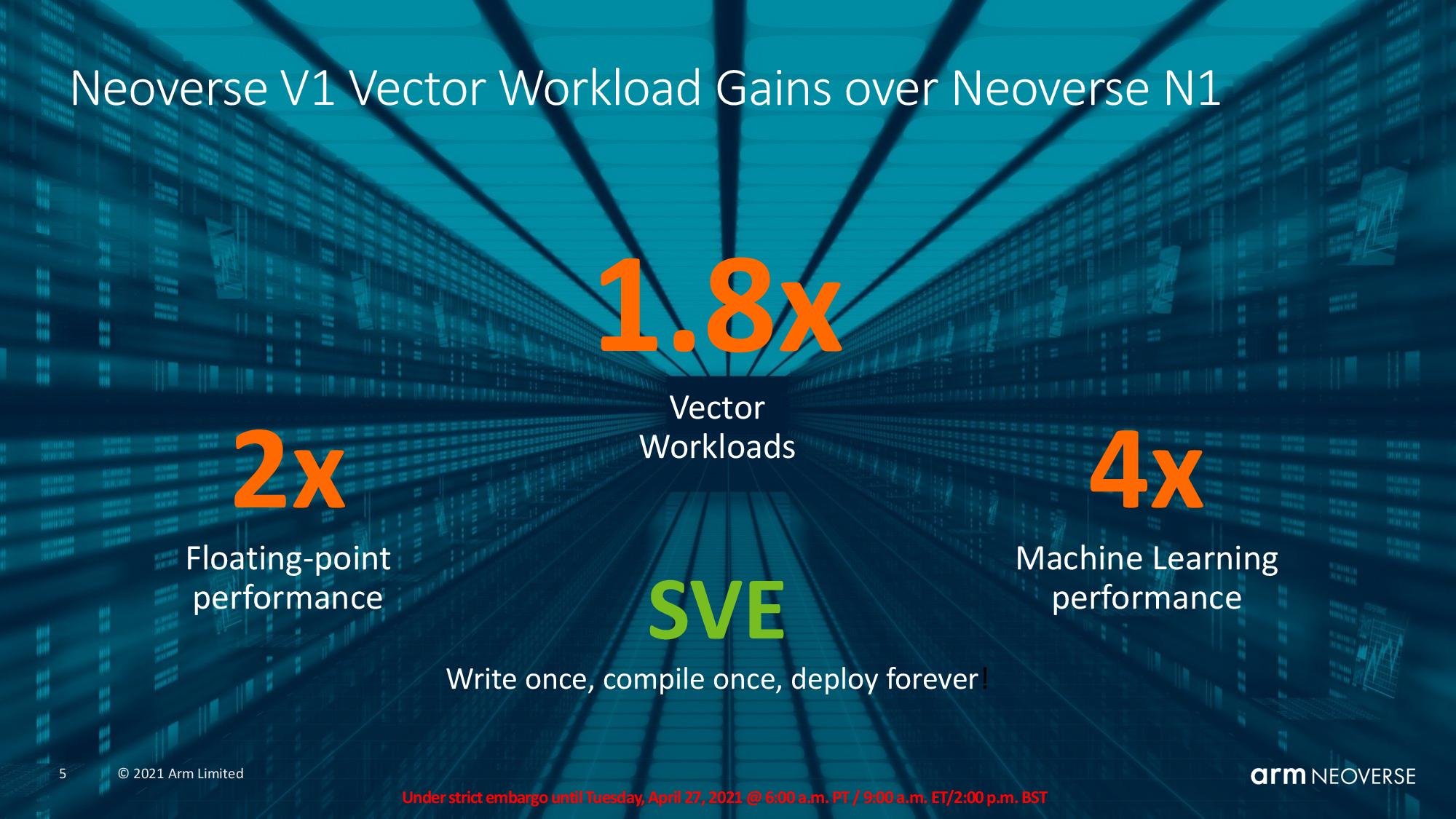
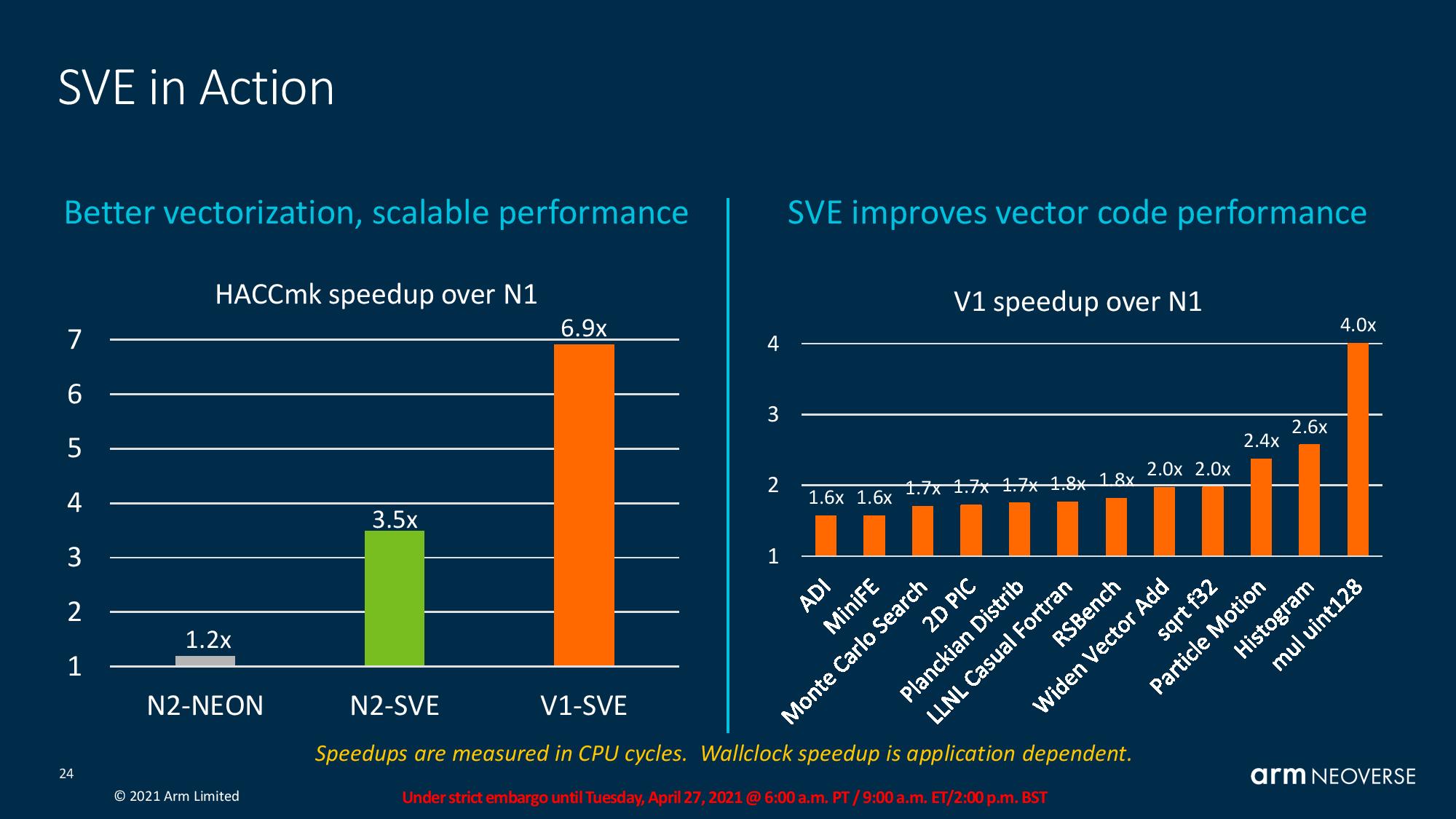
Additionally, Arm claims that, relative to the N1 platform, SVE contributes to a 2x increase in floating point performance, 1.8x increase in vectorized workloads, and 4x improvement in machine learning.
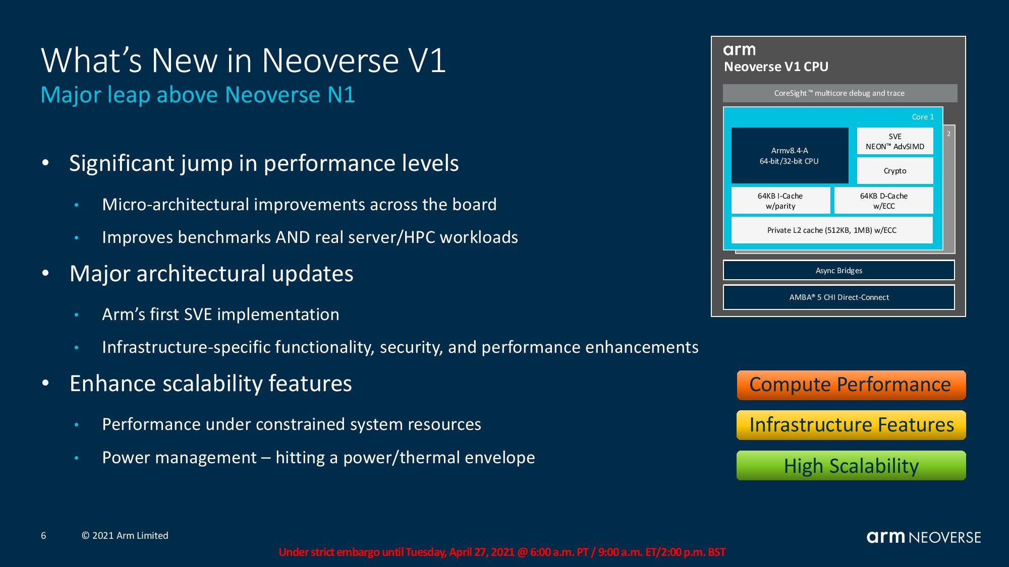
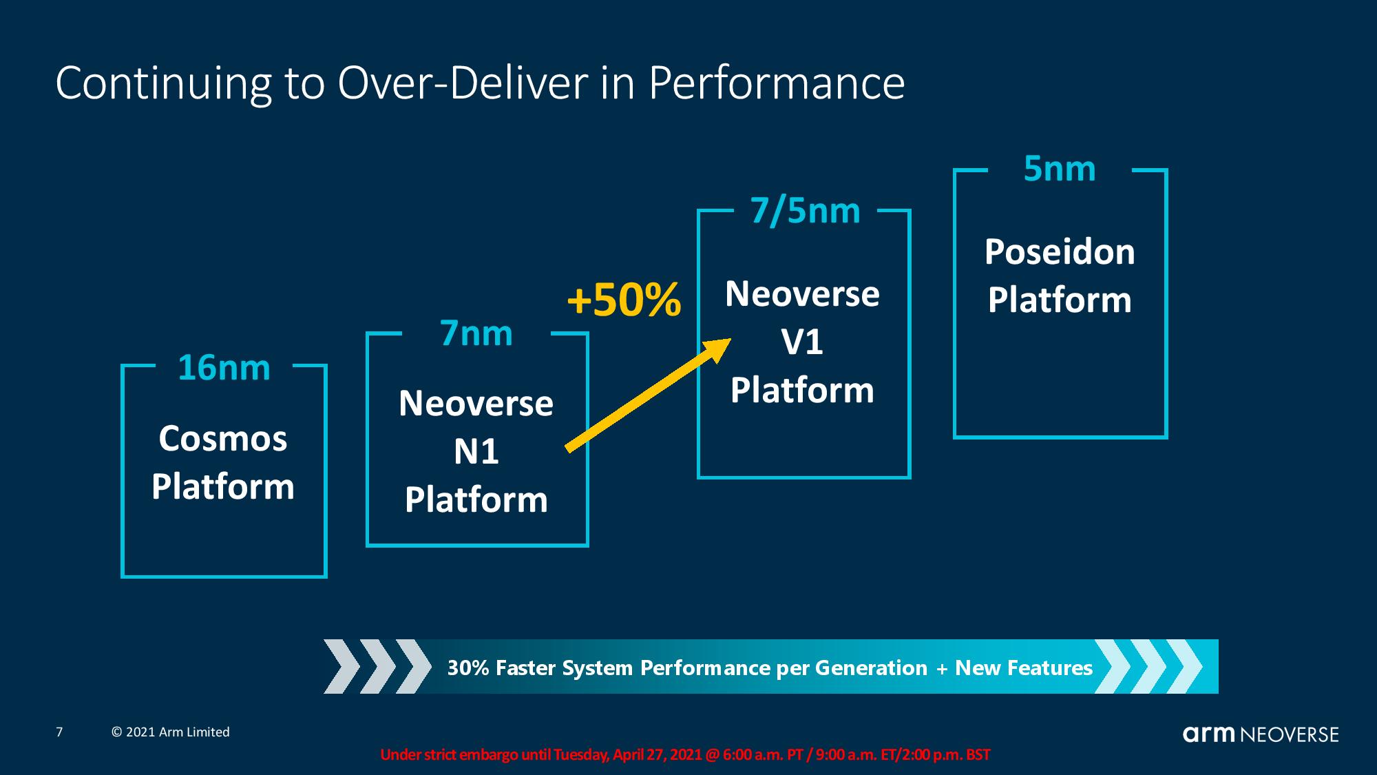
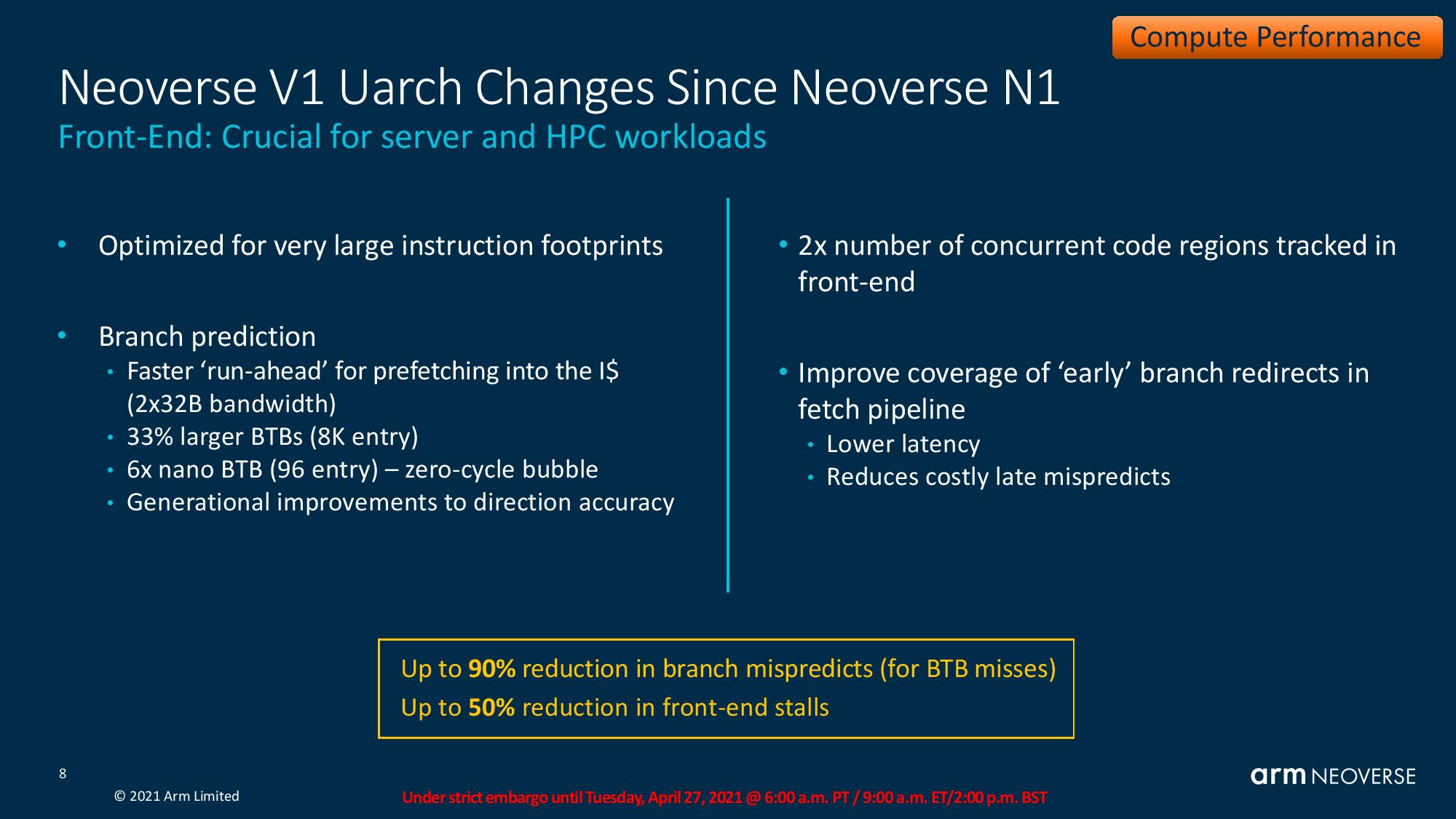
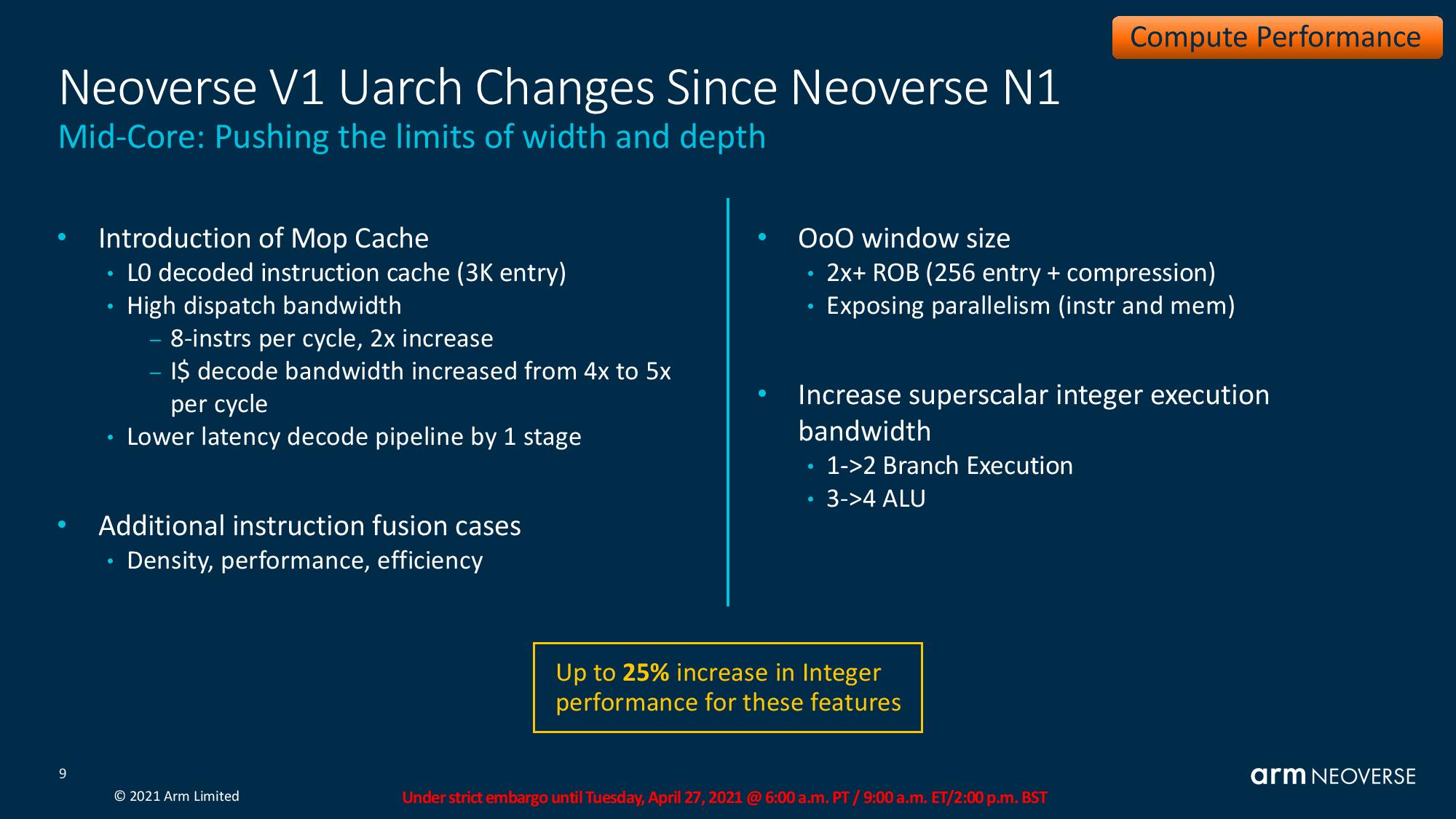
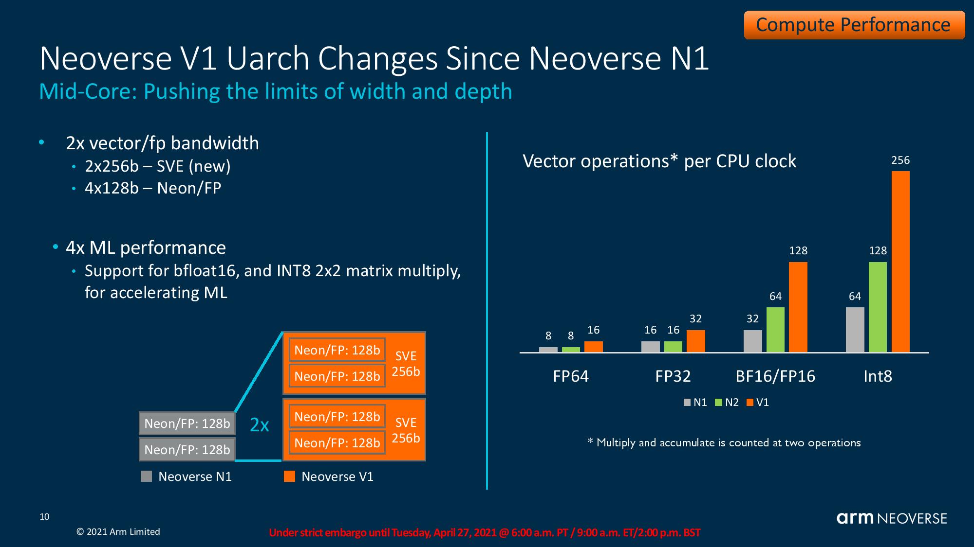
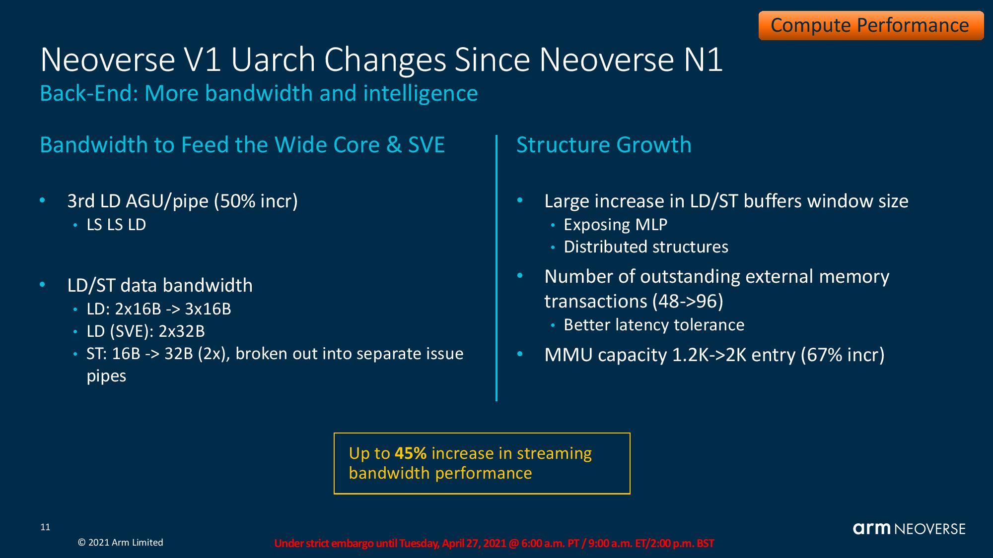
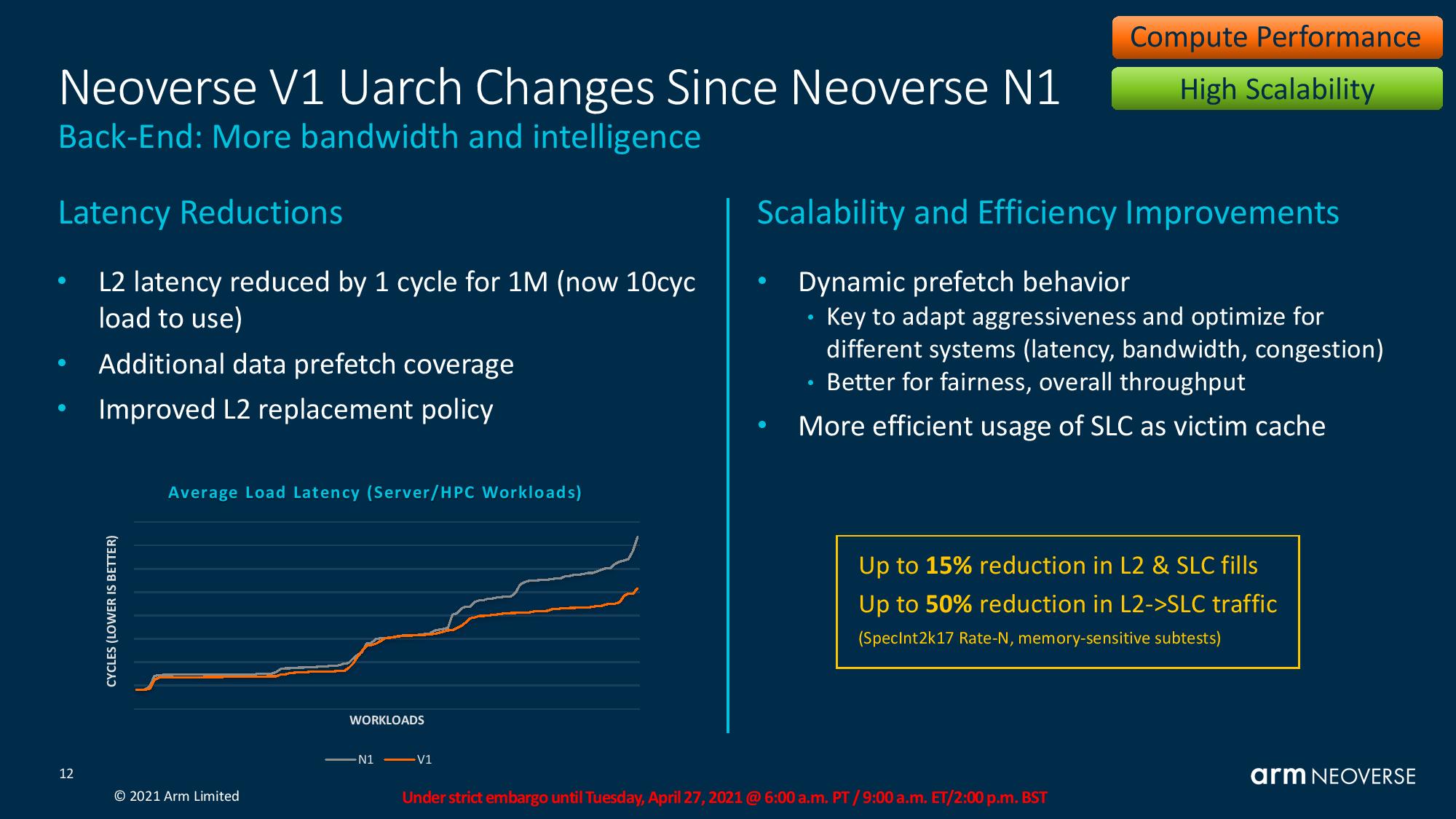
One of V1's biggest changes comes as the option to use either the 7nm or 5nm process, while the prior-gen N1 platform was limited to 7nm only. Arm also made a host of microarchitecture improvements spanning the front end, core, and back end to provide big speedups relative to prior-gen Arm chips, added support for SVE, and made accommodations to promote enhanced scalability.
Here's a bullet list of the biggest changes to the architecture. You can also find additional details in the slides above.
- Front End:
- Net of 90% reduction in branch mispredicts (for BTB misses) and a 50% reduction in front-end stalls
- V1 branch predictor decoupled from instruction fetch, so the prefetcher can run ahead and prefetch instruction into the instruction cache
- Widened branch prediction bandwidth to enable faster run-ahead to (2x32b per cycle)
- Increased capacity of the Dual-level BTB (Branch Target Buffers) to capture more branches with larger instruction footprints and to lower the taken branch latency, improved branch accuracy to reduce mispredicts
- Enhanced ability to redirect hard-to-predict branches earlier in the pipeline, at fetch time, for faster branch recovery, improving both performance and power
- Mid-Core:
- Net increase of 25% in integer performance
- Micro-Op (MOP) Cache: L0 decoded instruction cache optimizes the performance of smaller kernels in the microarchitecture, 2x increase in fetch and dispatch bandwidth over N1, lower-latency decode pipeline by removing one stage
- Added more instruction fusion capability, improves performance end power efficiency for most commonly-used instruction pairs
- OoO (Out of Order) window increase by 2X to enhance parallelism. Also increased integer execution bandwidth with a second branch execution unit and a fourth ALU
- SIMD and FP Units: Added a new SVE implementation — 2x256b operations per cycle. Doubled raw execute capability from 2x128b pipelines in N1 to 4x128b in V1. Slide 10 — 4x improvement in ML performance
- Back End:
- 45% increase to streaming bandwidth by increasing load/store address bandwidth by 50%, adding a third load data address generation unit (AGU - 50% increase)
- To improve SIMD and integer floating point execution, added a third load data pipeline and improved load bandwidth for integer and vector. Doubled store bandwidth and split scheduling into two pipes
- Load/store buffer window sizes increased. MMU capacity, allow for a larger number of cache translations
- Reduce latencies in L2 cache to improve single-threaded performance (slide 12)
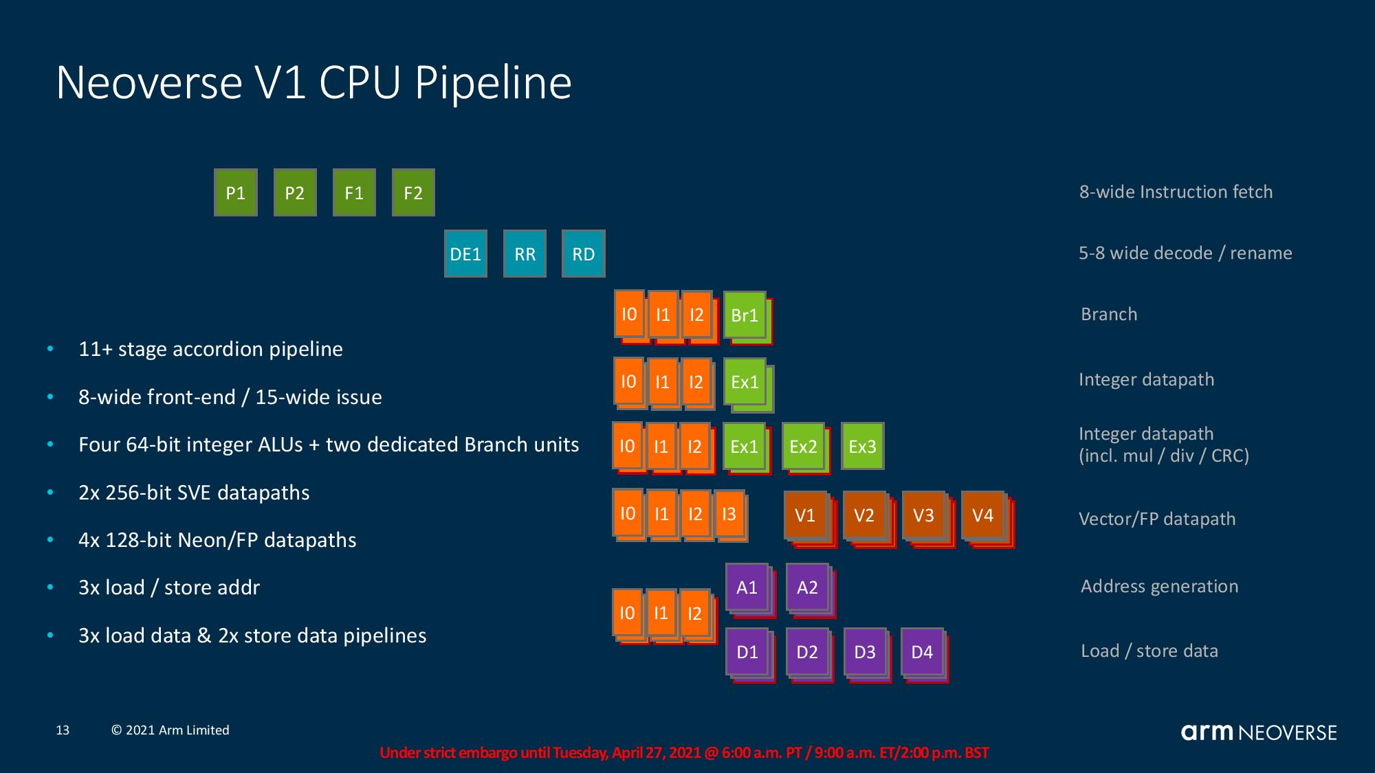
This diagram shows the overall pipeline depth (left to right) and bandwidth (top to bottom), highlighting the impressive parallelism of the design.

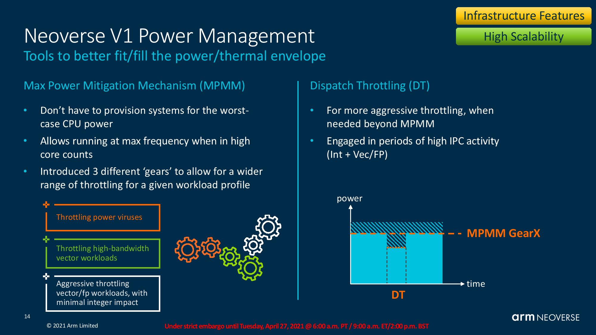
Arm also instituted new power management and low-latency tools to extend beyond the typical capabilities of Dynamic Voltage Frequency Scaling (DVFS). These include the Max Power Mitigation Mechanism (MPMM) that provides a tunable power management system that allows customers to run high core-count processors at the highest possible frequencies, and Dispatch Throttling (DT), which reduces power during certain workloads with high IPC, like vectorized work (much like we see with Intel reducing frequency during AVX workloads).
At the end of the day, it's all about Power, Performance, and Area (PPA), and here Arm shared some projections. With the same (ISO) process, Arm claims up to 1.5x IPC increase over the previous-gen N1 and a 70% to 100% improvement to power efficiency (varies by workload). Given the same L1 and L2 cache sizes, the V1 core is 70% larger than the N1 core.
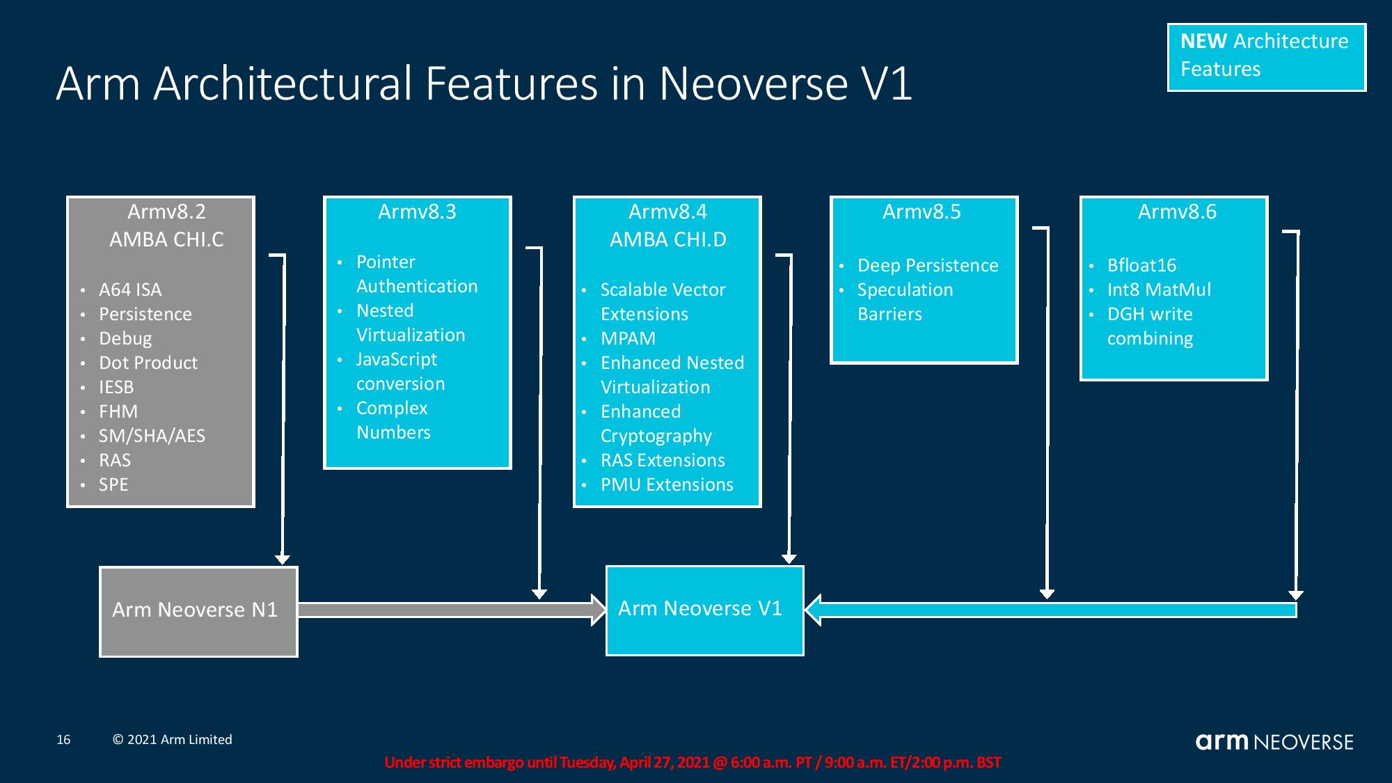
The Neoverse V1 supports Armv8.4, but the chip also borrows some features from future v8.5 and v8.6 revisions, as shown above.
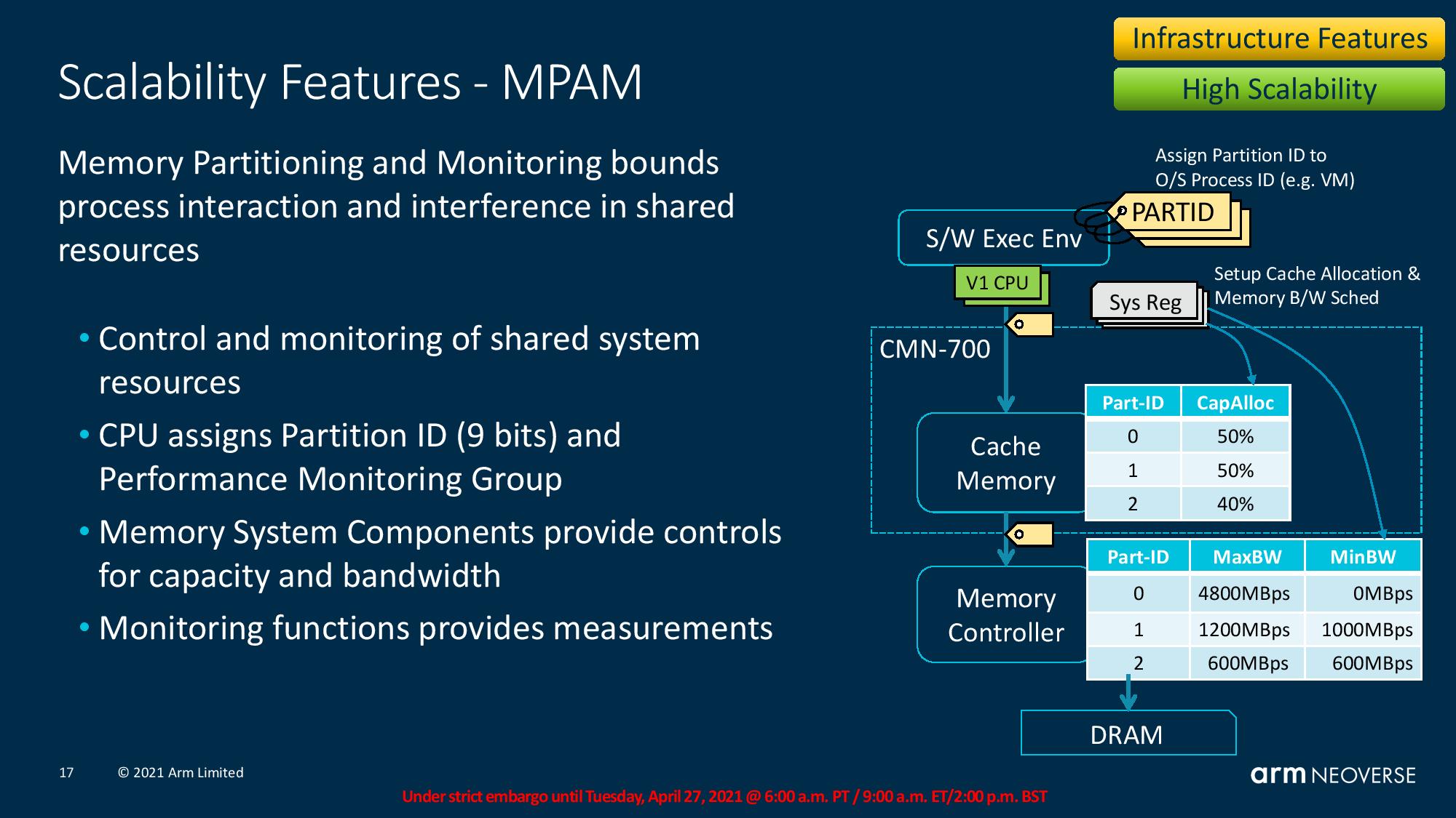
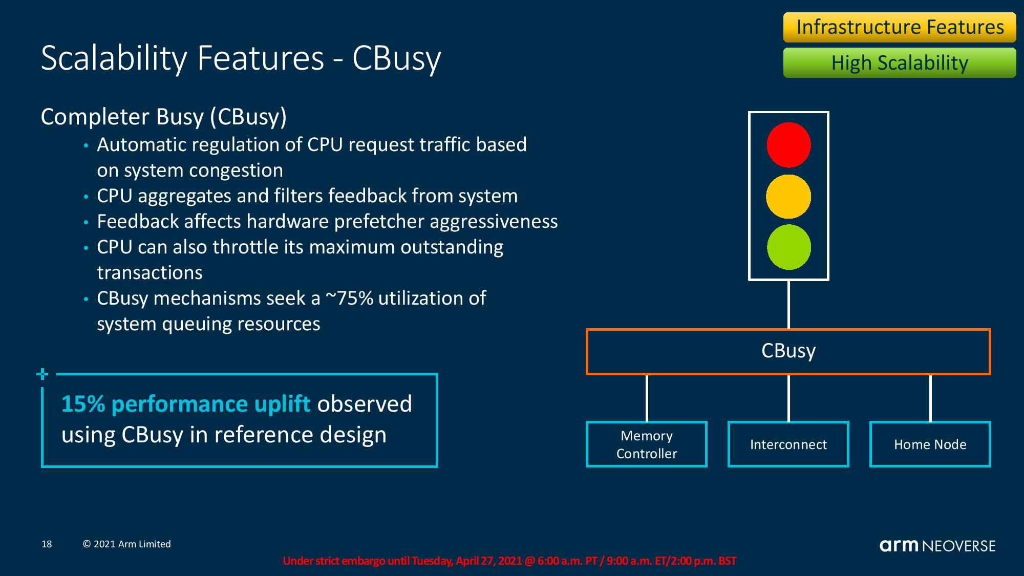
Arm also added several features to manage system scalability, particularly as it pertains to partitioning shared resources and reducing contention, as you can see in the slides above.
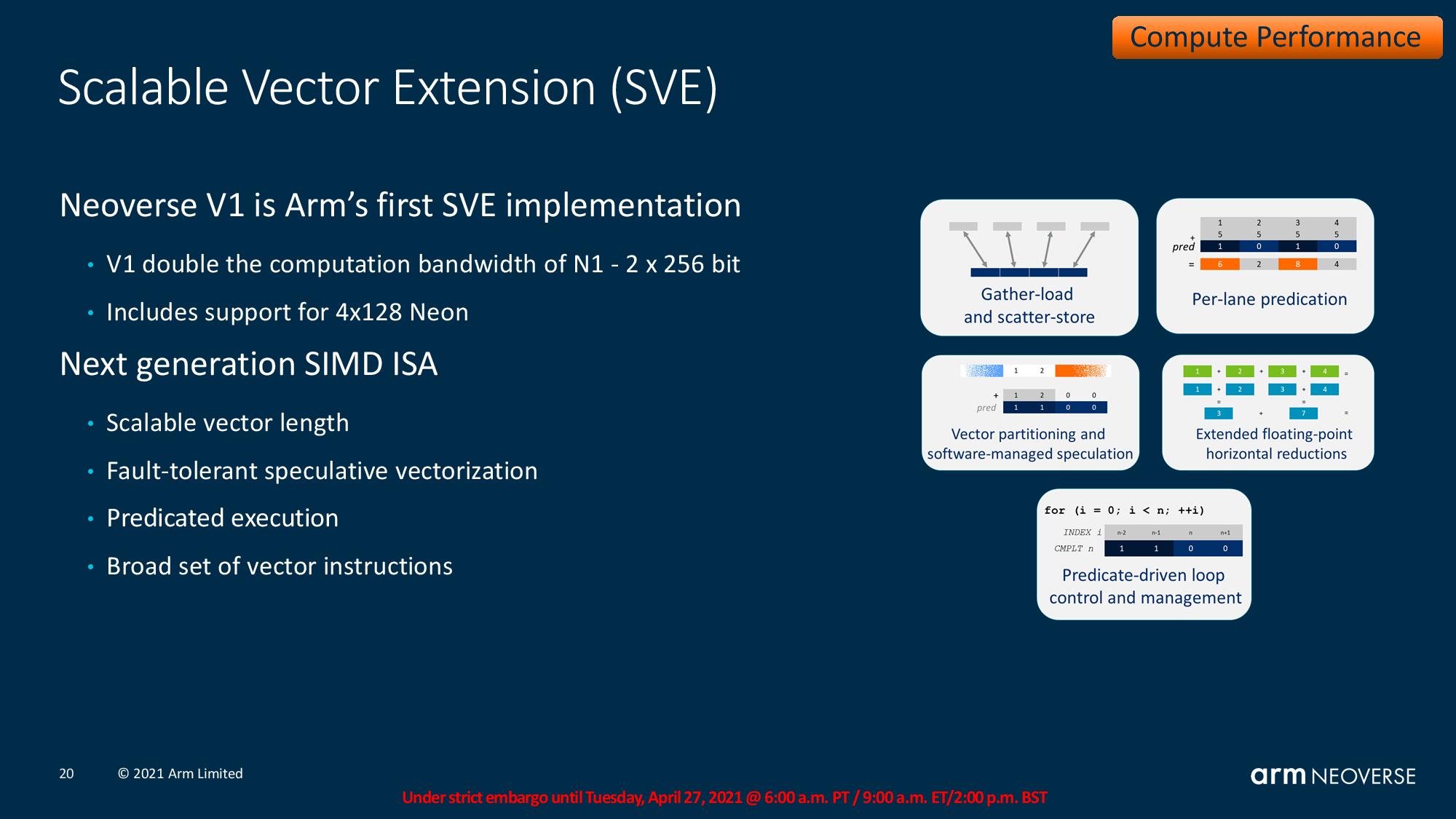
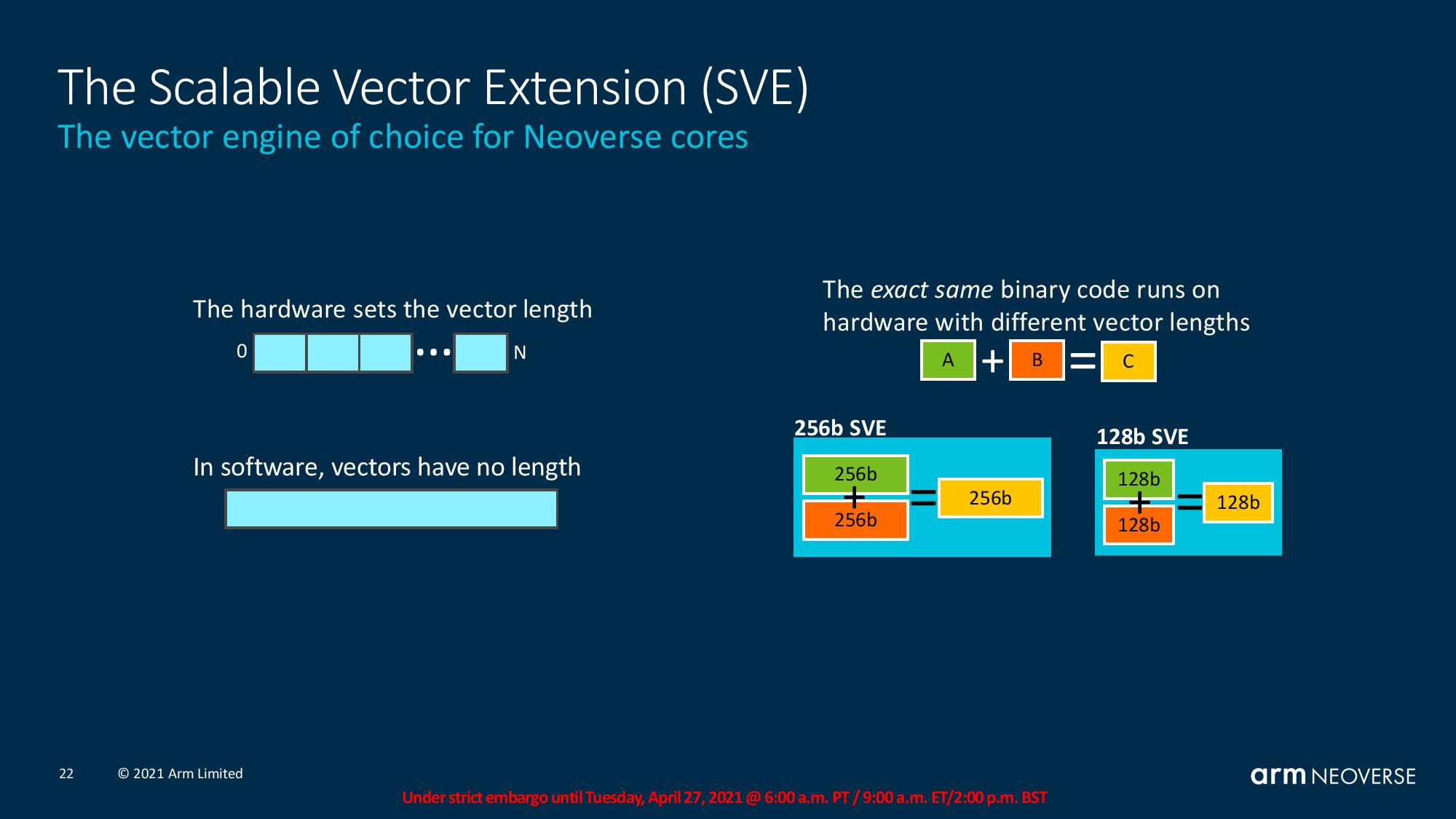
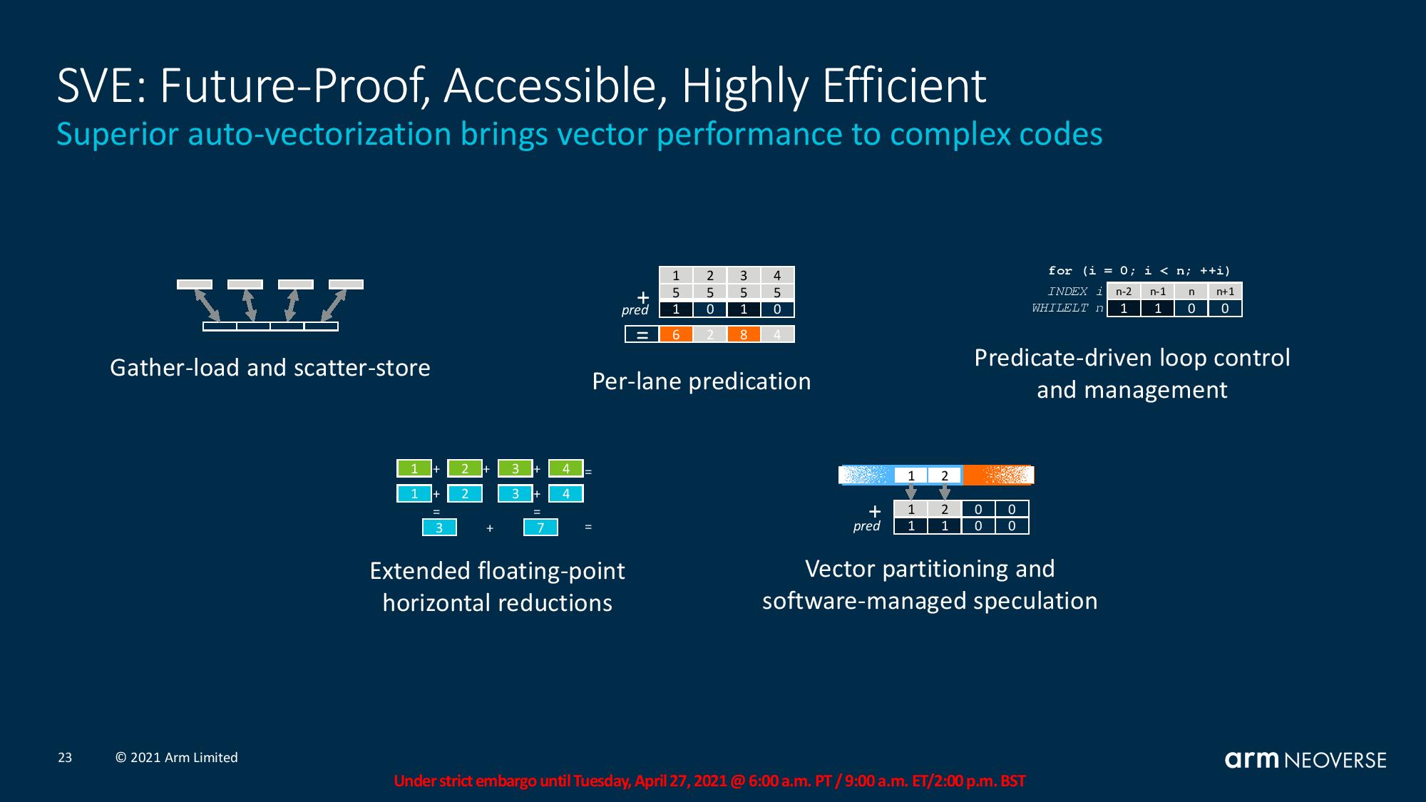
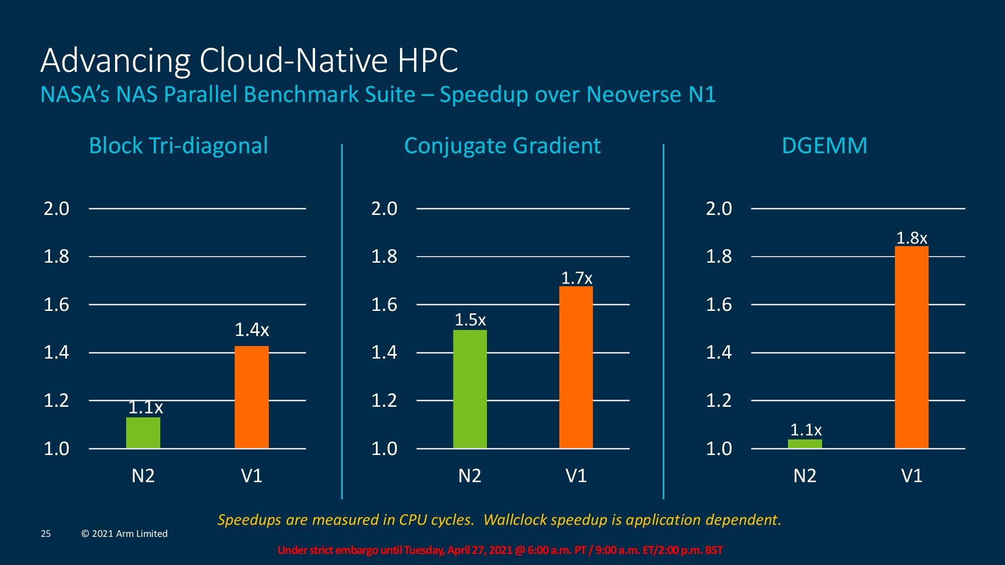
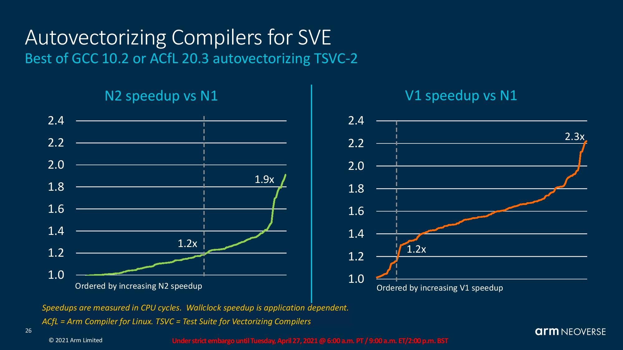
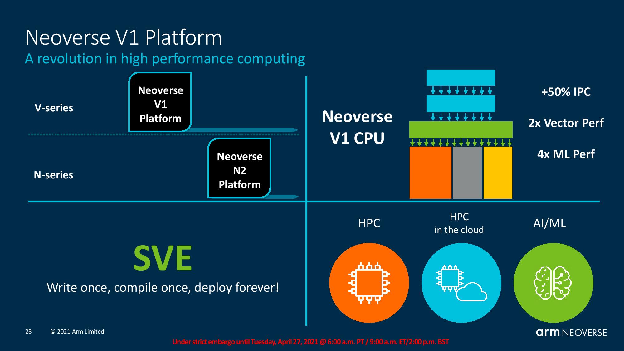
Arm's Scalable Vector Extensions (SVE) are a big draw of the new architecture. Firstly, Arm doubled compute bandwidth to 2x256b with SVE and provides backward support for Neon at 4x128b.
However, the key here is that SVE is vector length agnostic. Most vector ISAs have a fixed number of bits in the vector unit, but SVE lets the hardware set the vector length in bits. However, in software, the vectors have no length. This simplifies programming and enhances portability for binary code between architectures that support different bit widths — the instructions will automatically scale as necessary to fully utilize the available vector bandwidth (for instance, 128b or 256b).
Arm shared information on several fine-grained instructions for the SVE instructions, but much of those details are beyond the scope of this article. Arm also shared some simulated V1 and N2 benchmarks with SVE, but bear in mind that these are vendor-provided and merely simulations.
ARM Neoverse N2 Platform 'Perseus'
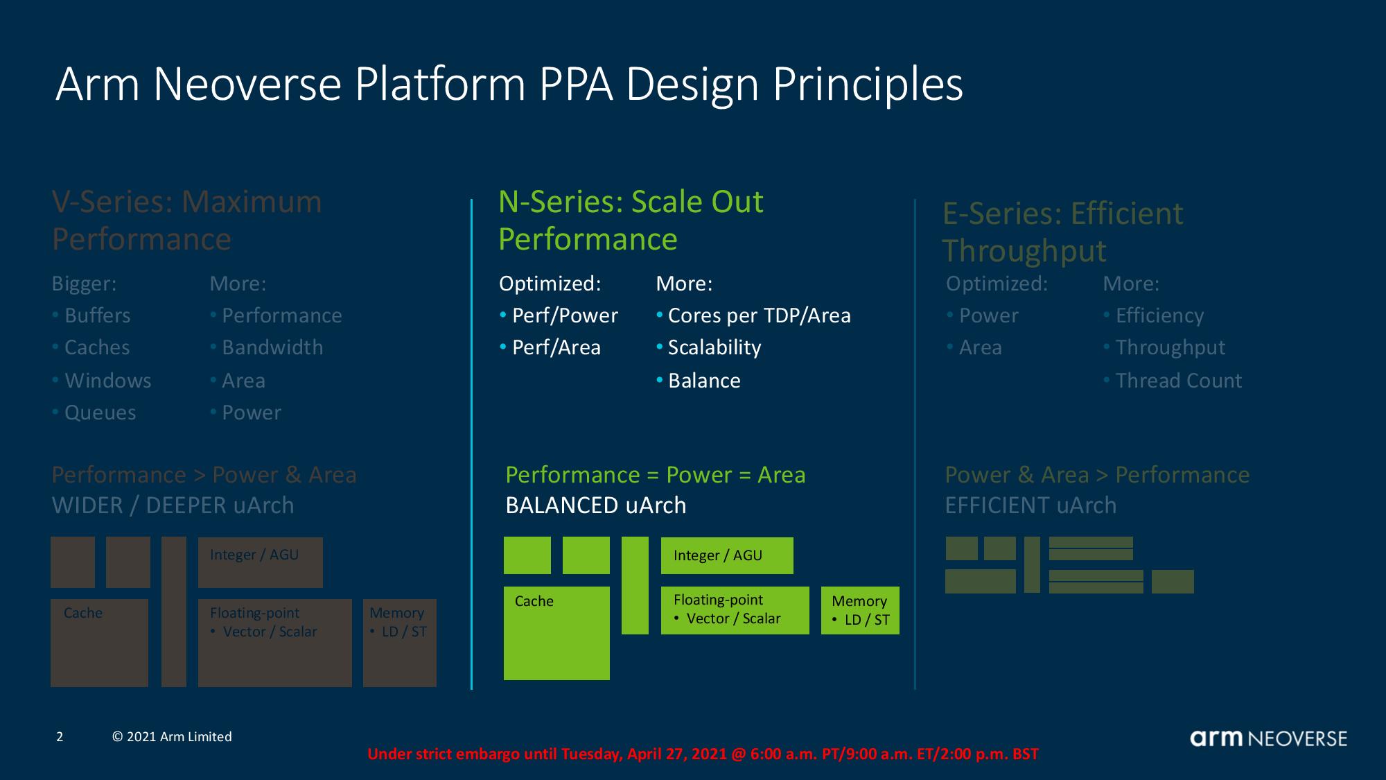
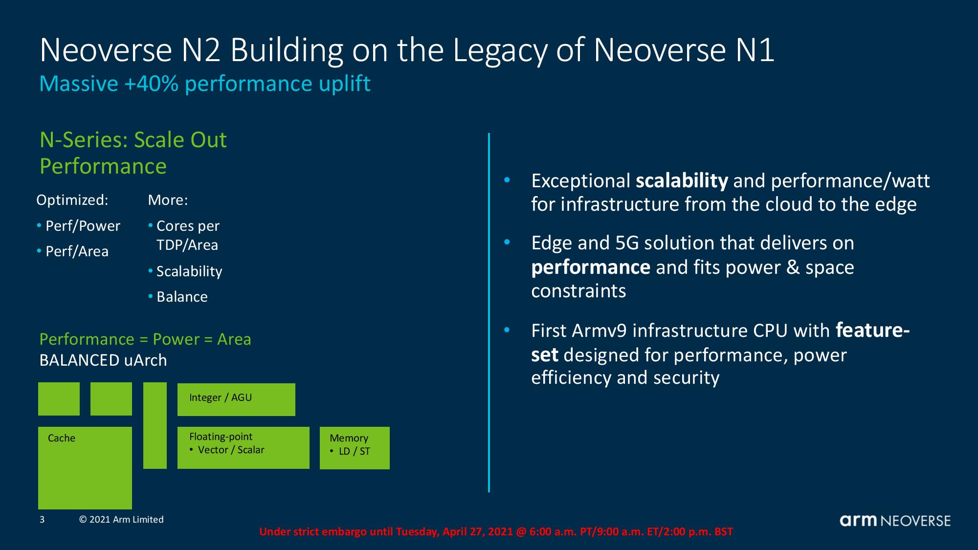
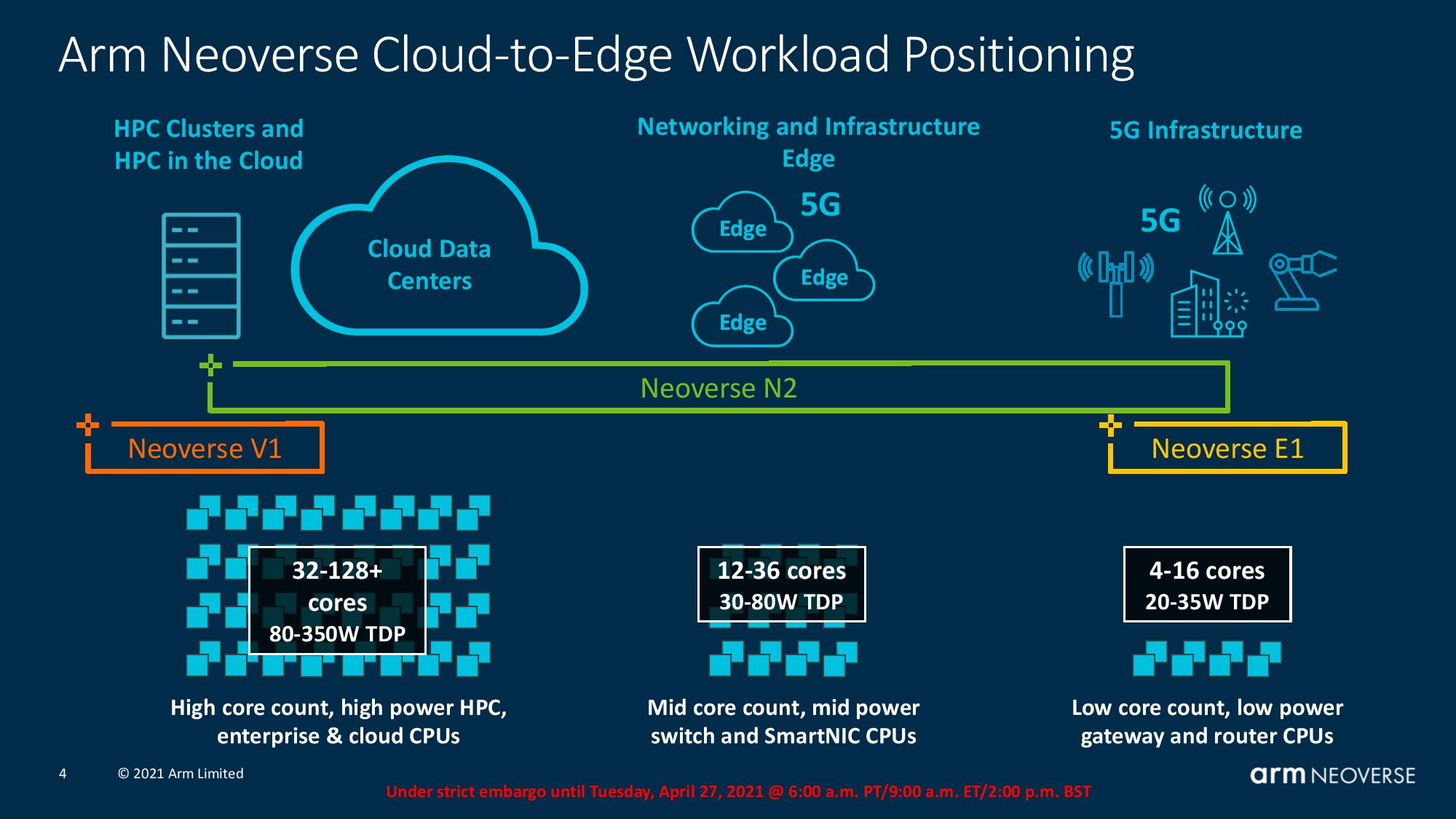
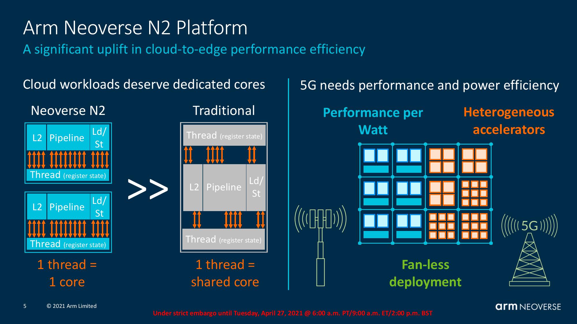
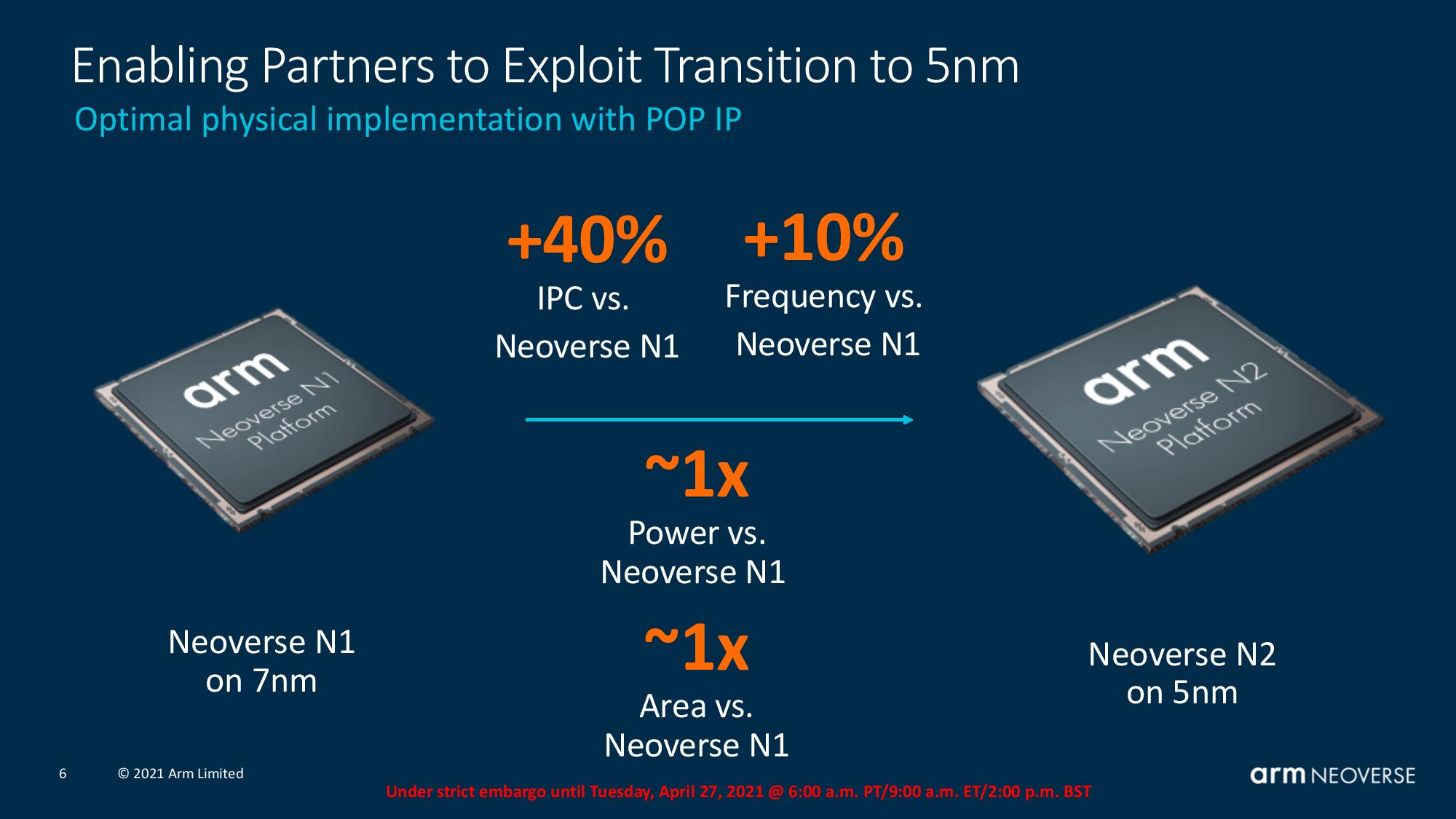
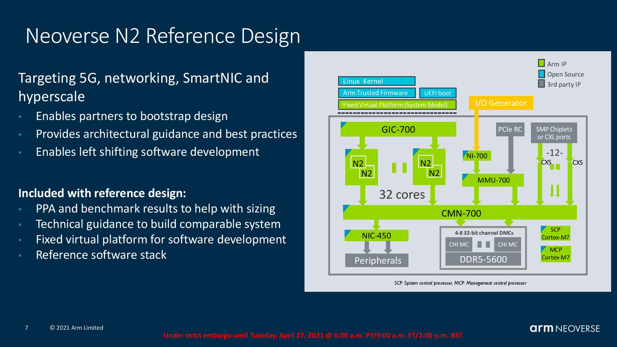
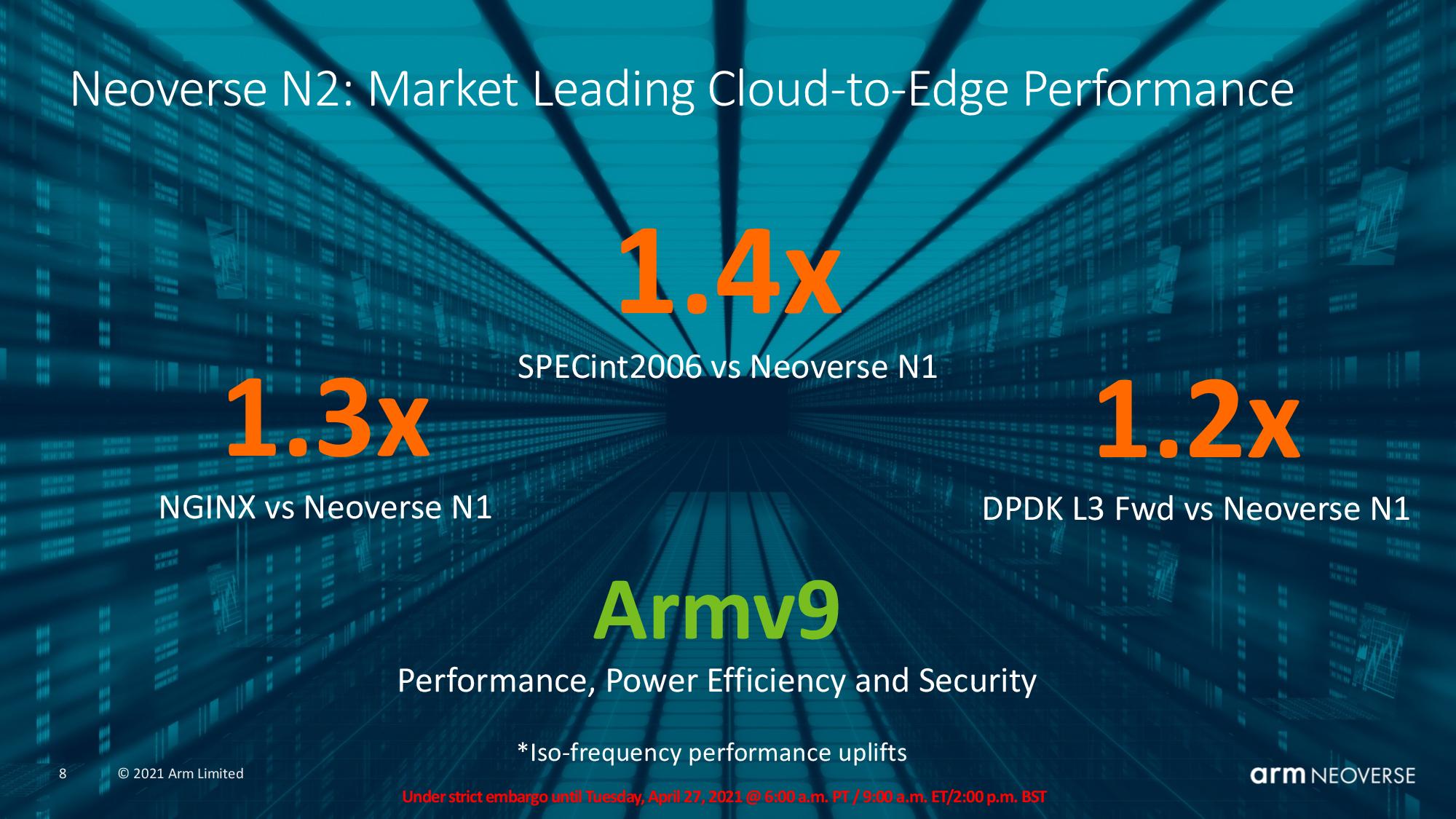
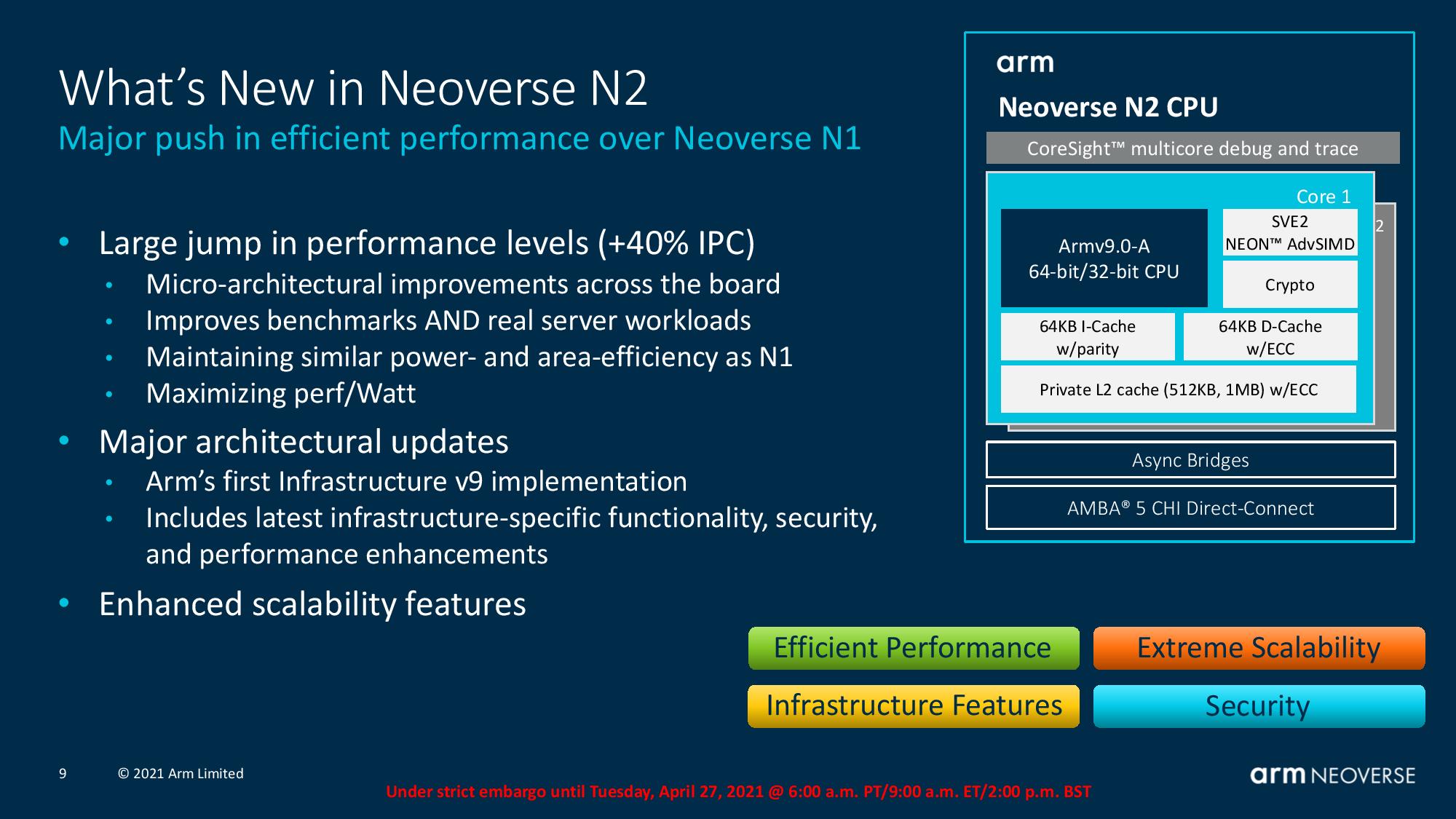
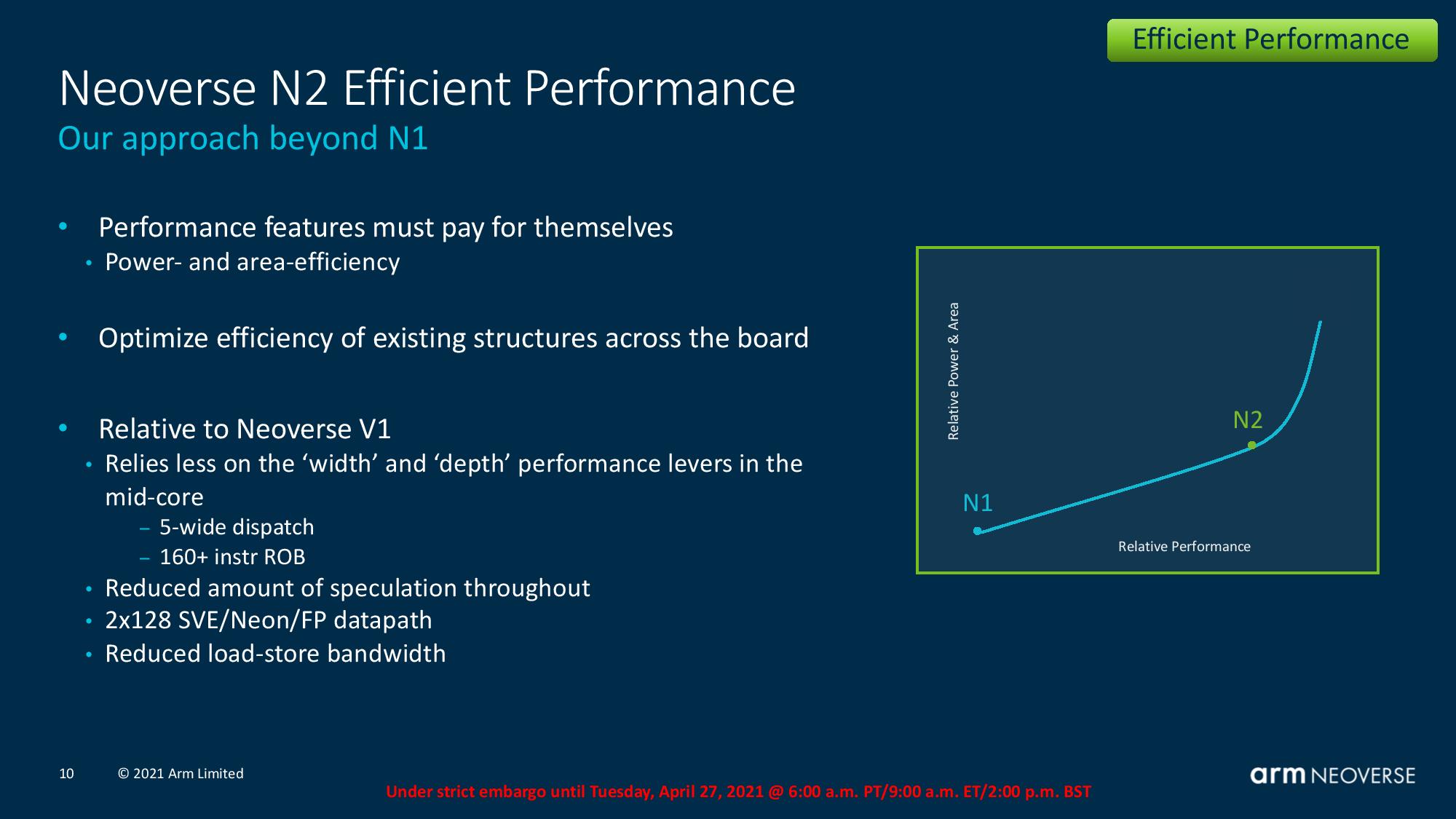
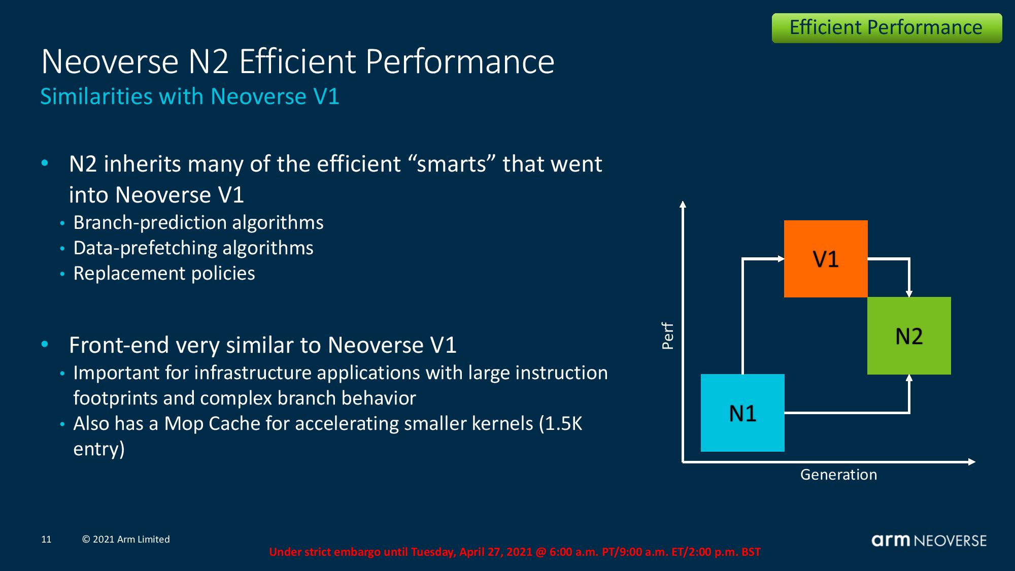
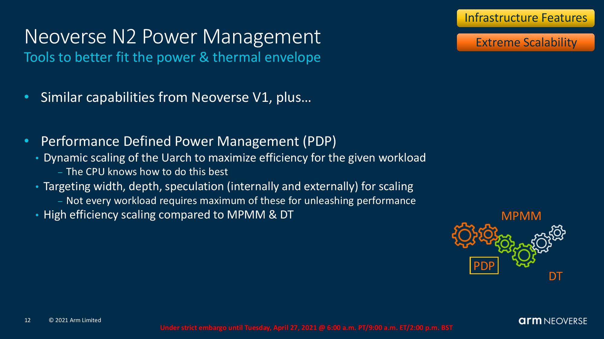
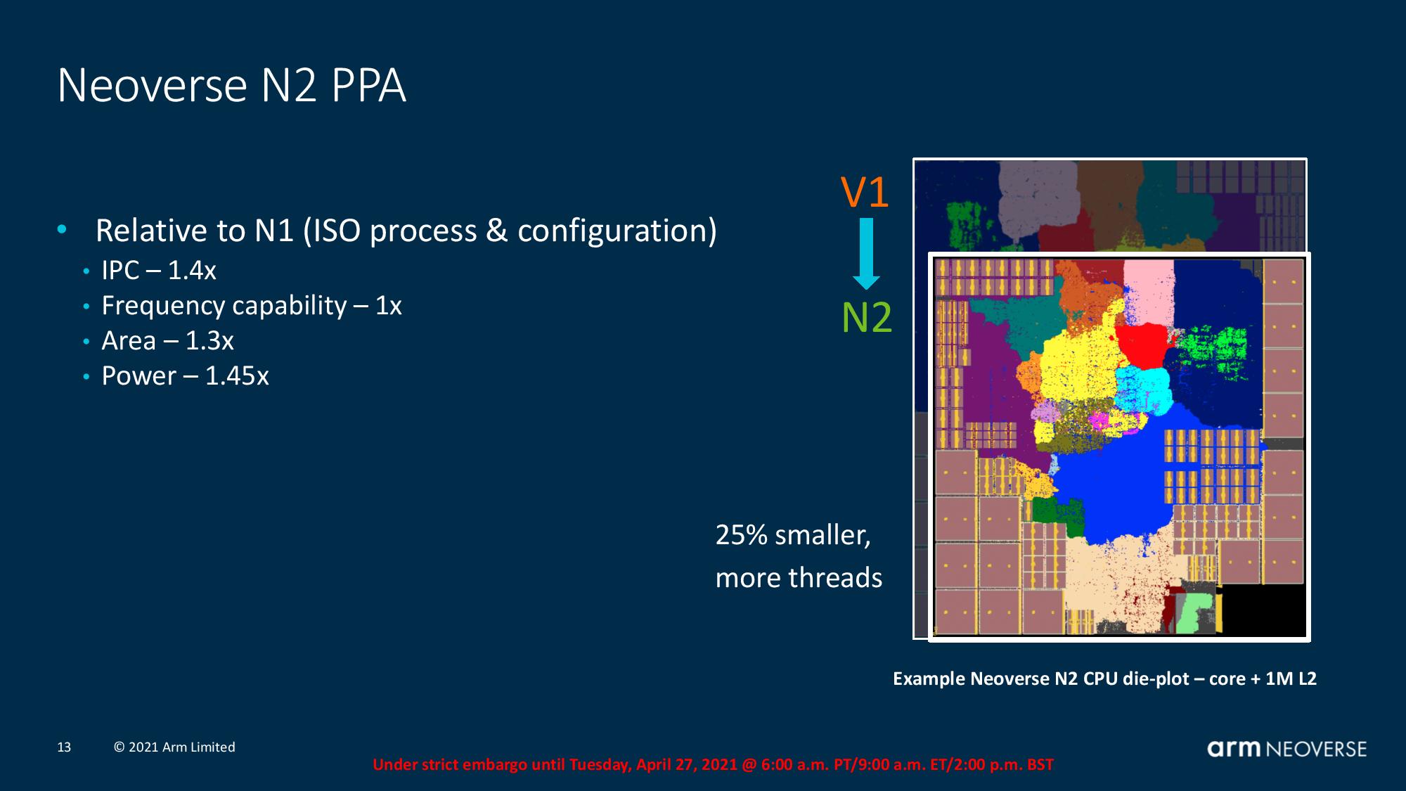
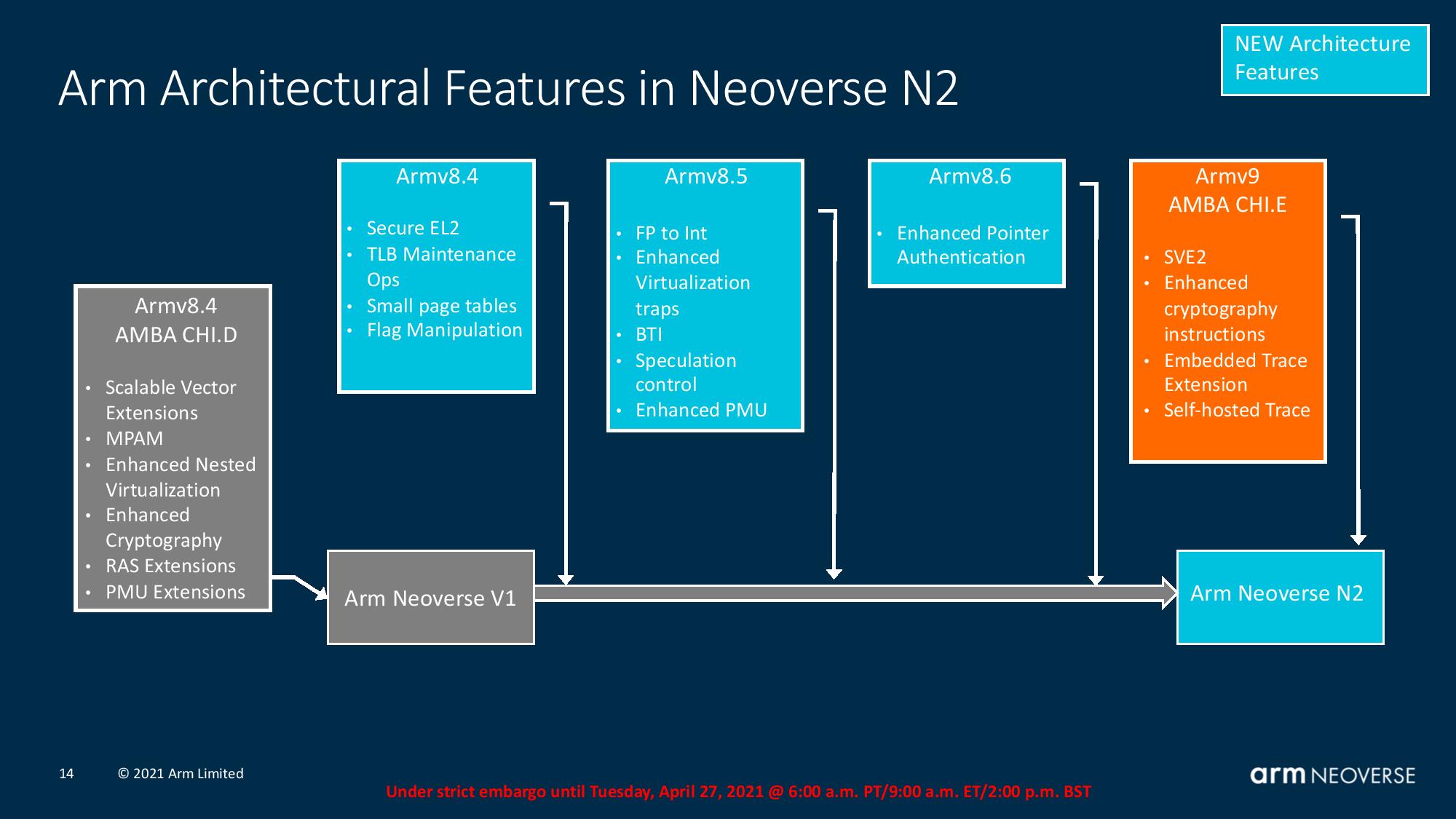
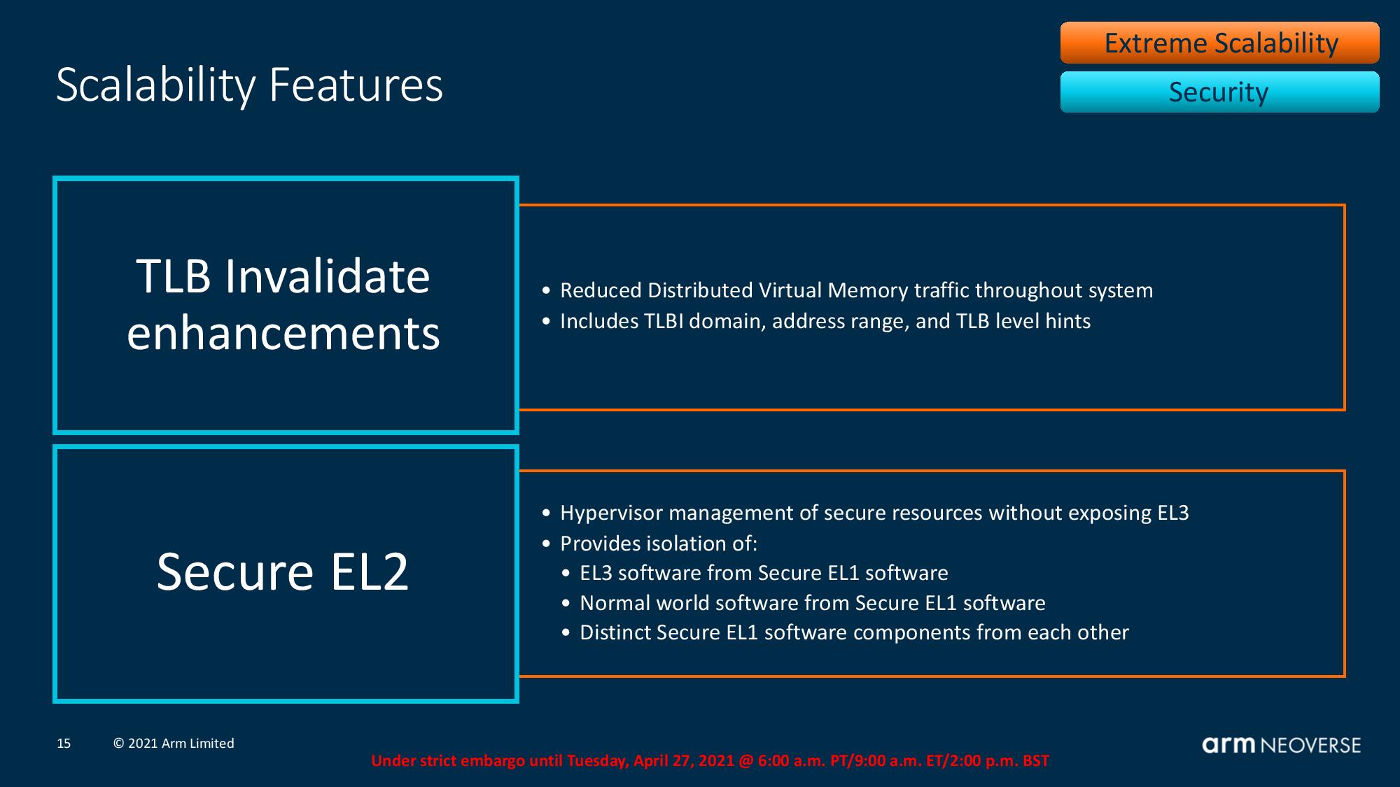
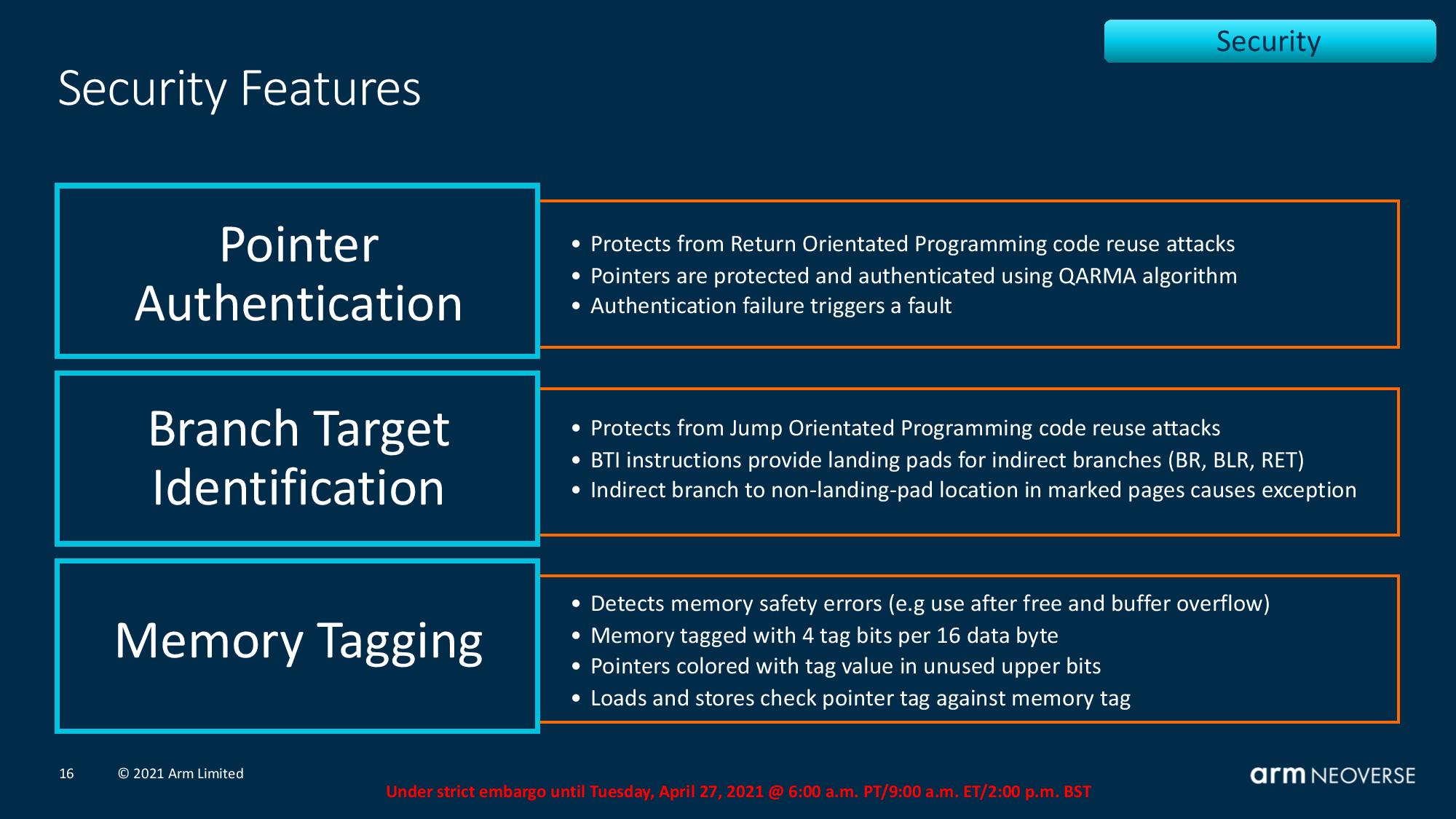
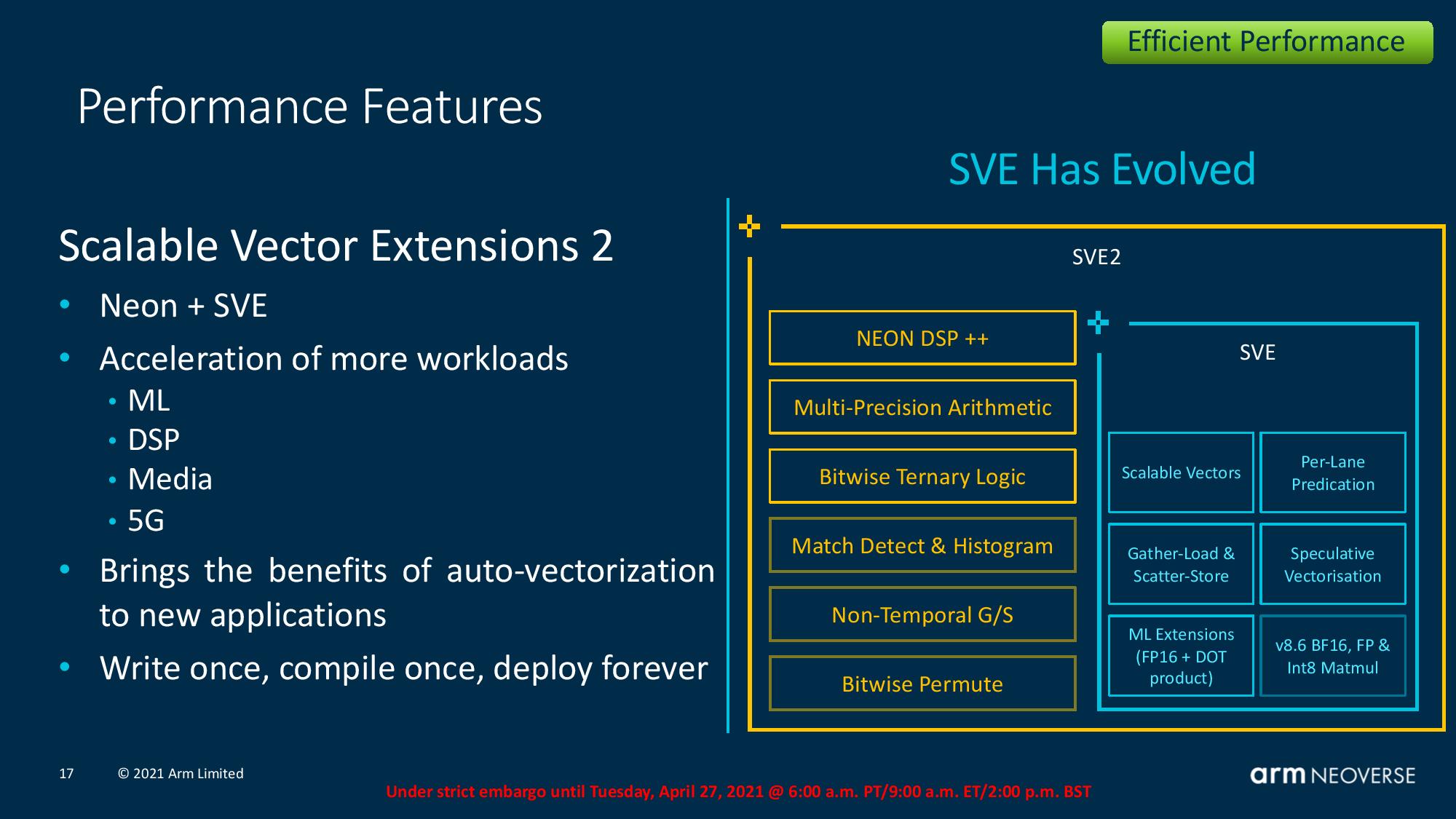
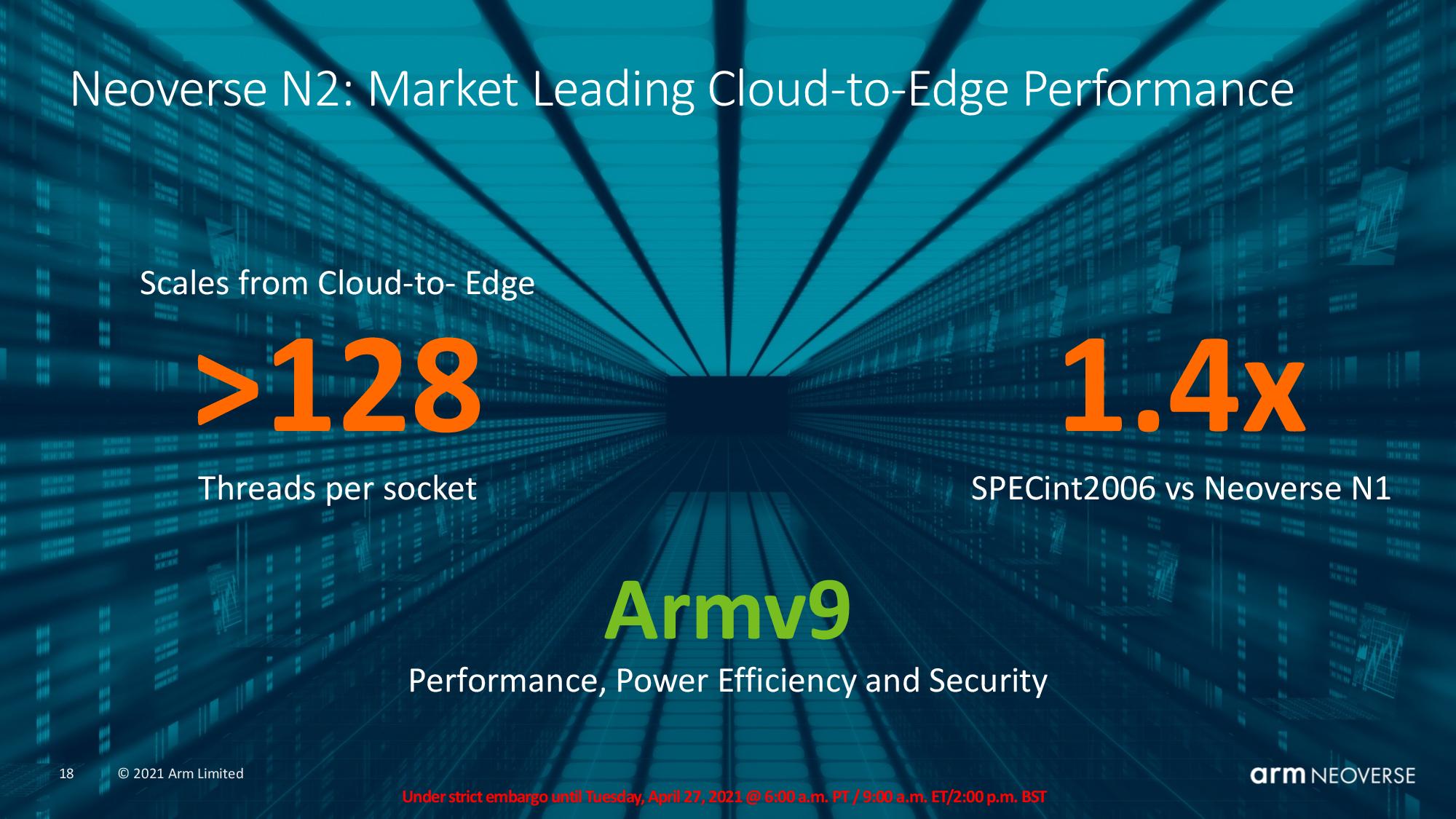
Here we can see the slide deck for the N2 Perseus platform, with the key goals being a focus on scale-out implementations. Hence, the company optimized the design for performance-per-power (watt) and performance-per-area, along with a healthier dose of cores and scalability. As with the previous-gen N1 platform, this design can scale from the cloud to the edge.
Neoverse N2 has a newer core than the V1 chips, but the company isn't sharing many details yet. However, we do know that N2 is the first Arm platform to support Armv9 and SVE2, which is the second generation of the SVE instructions we covered above.
Arm claims a 40% increase in single-threaded performance over N1, but within the same power and area efficiency envelope. Most of the details about N2 mirror those we covered with V1 above, but we included the slides above for more details.
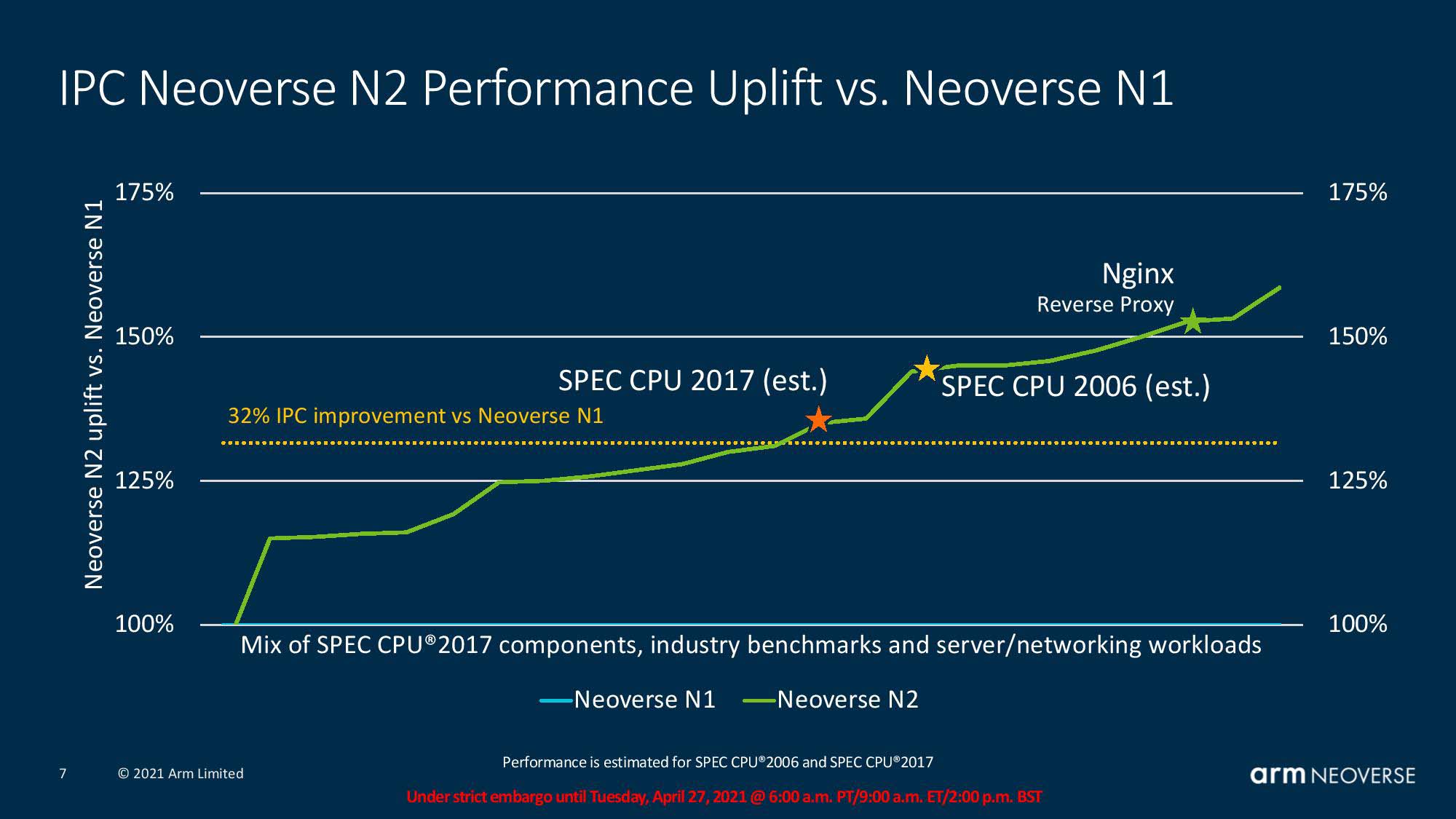
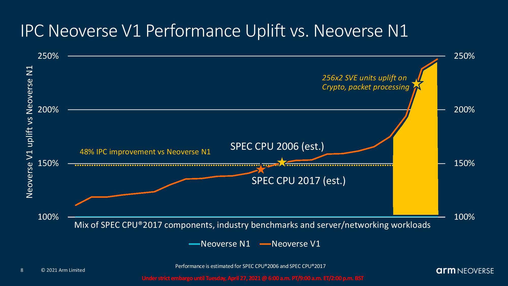
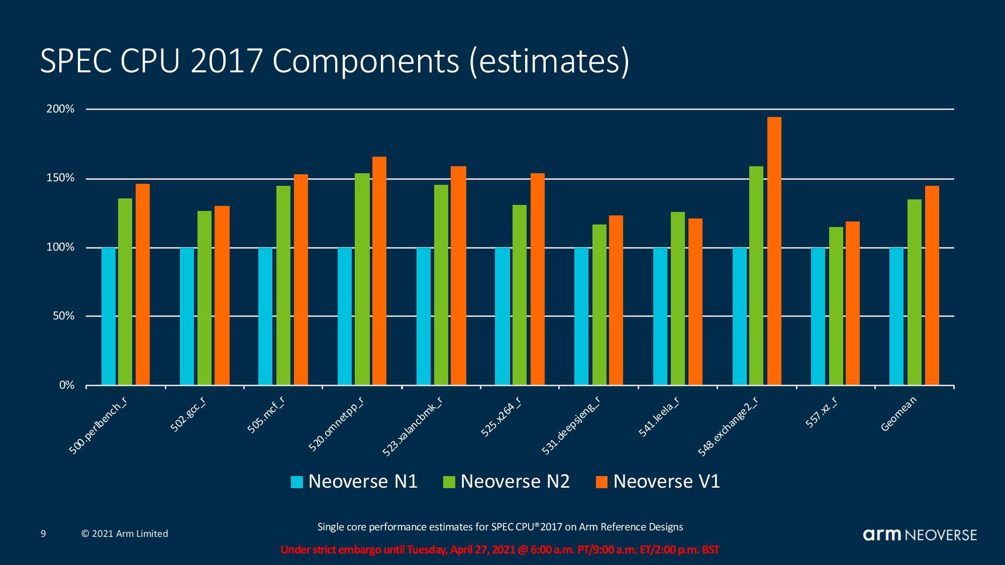
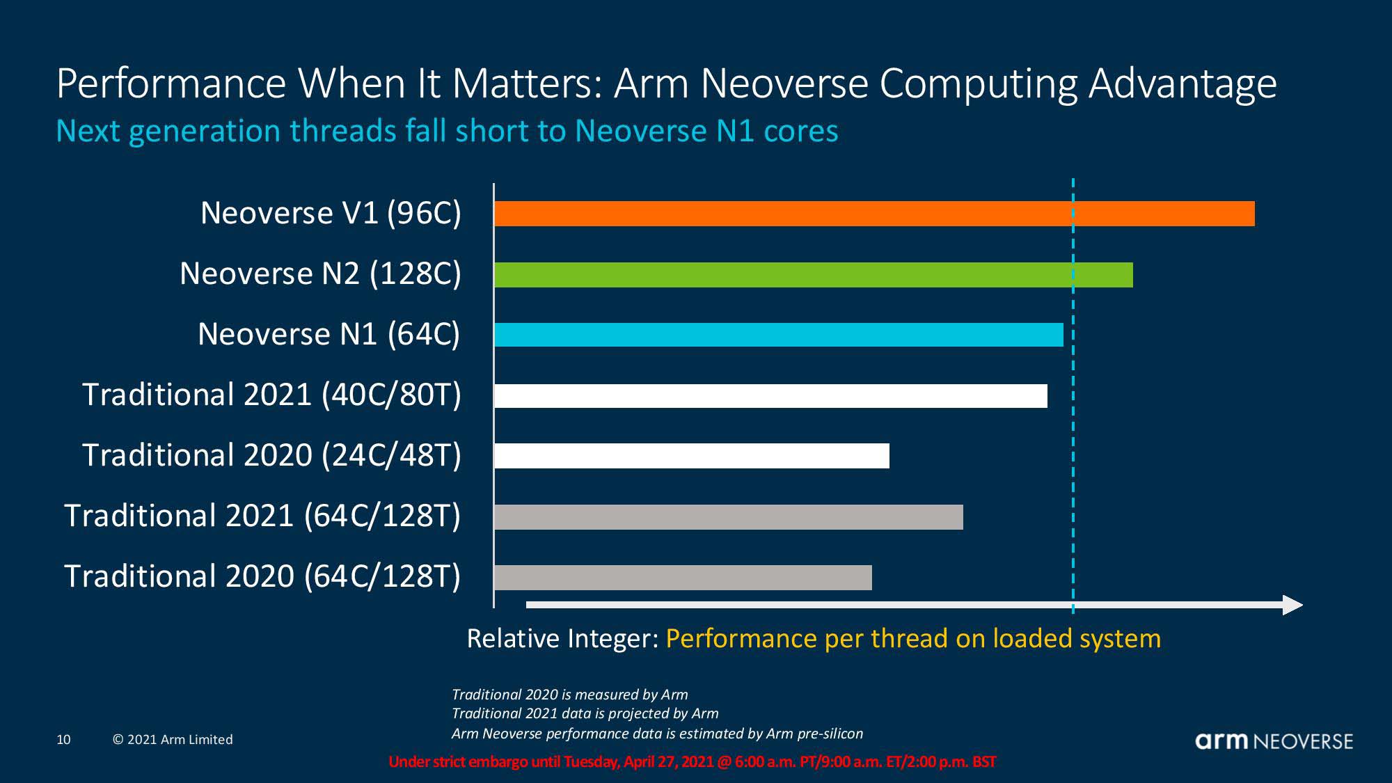
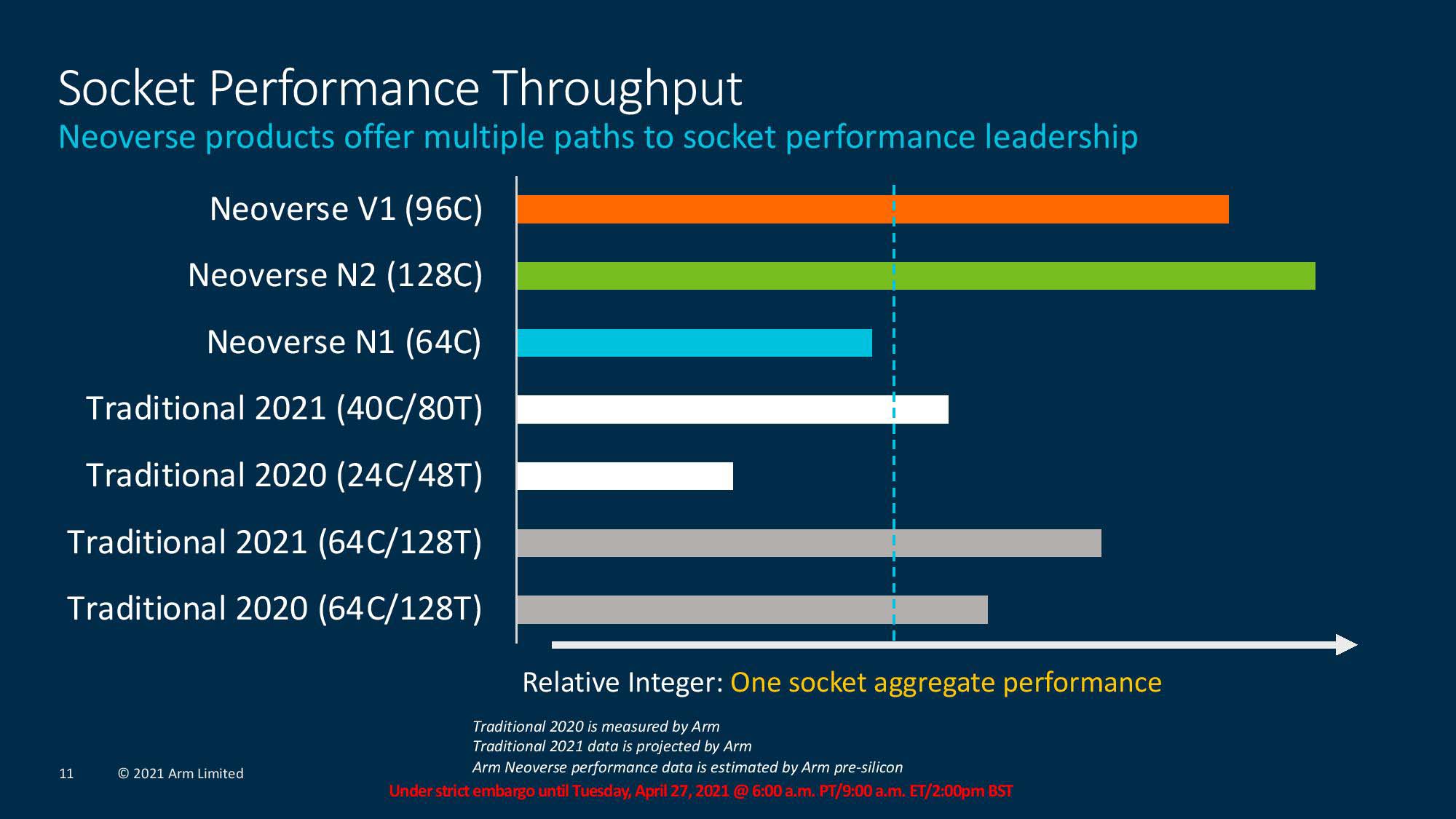
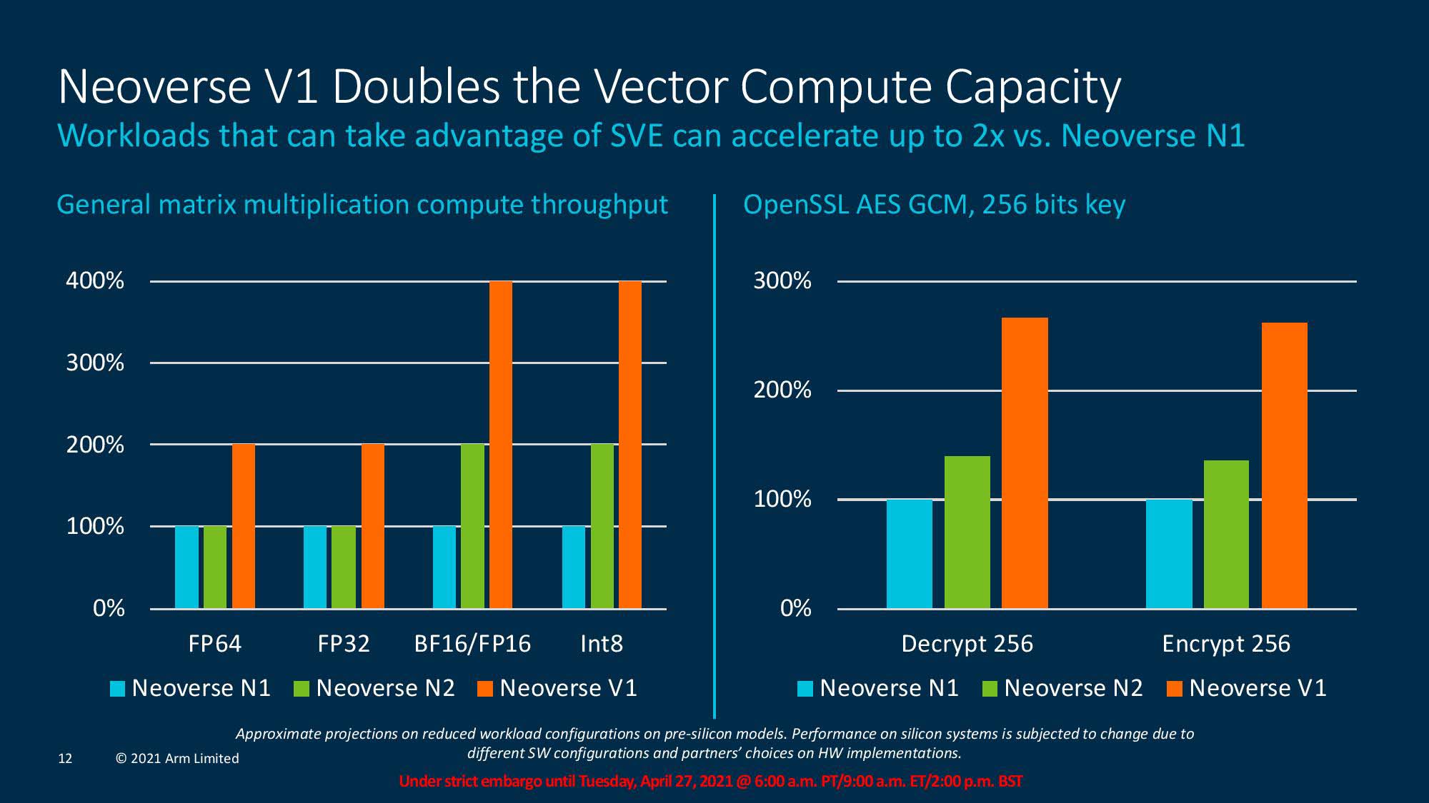
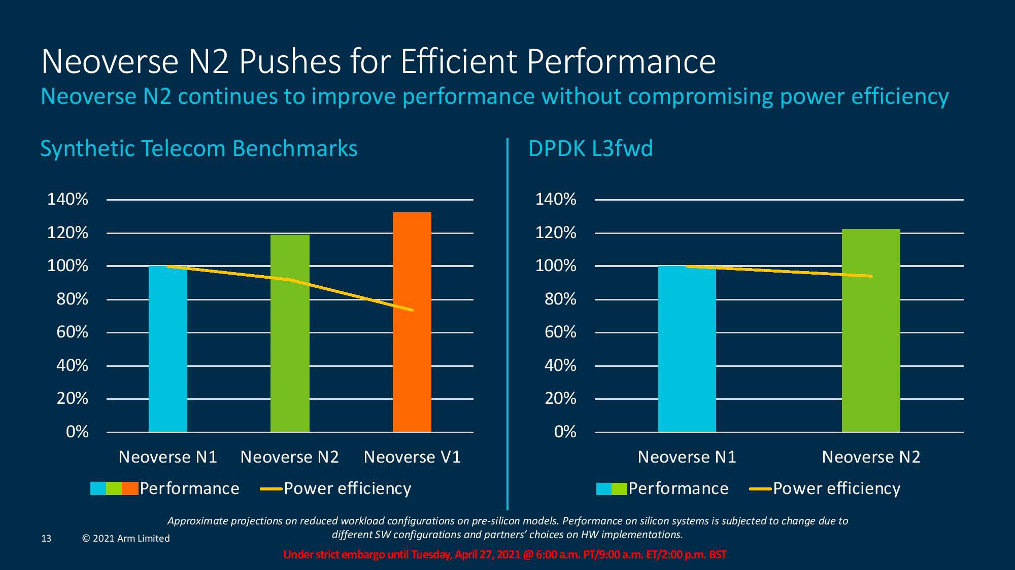
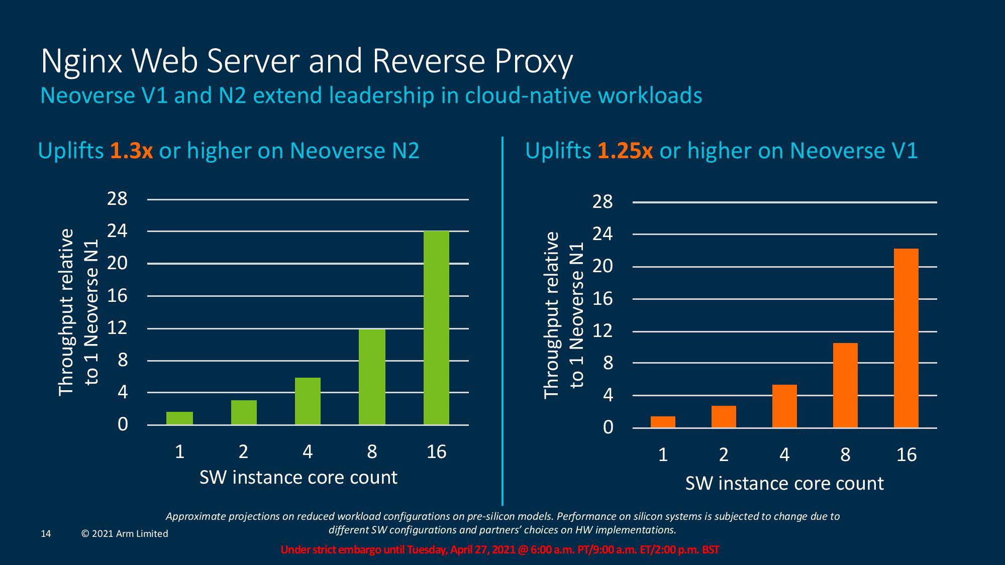
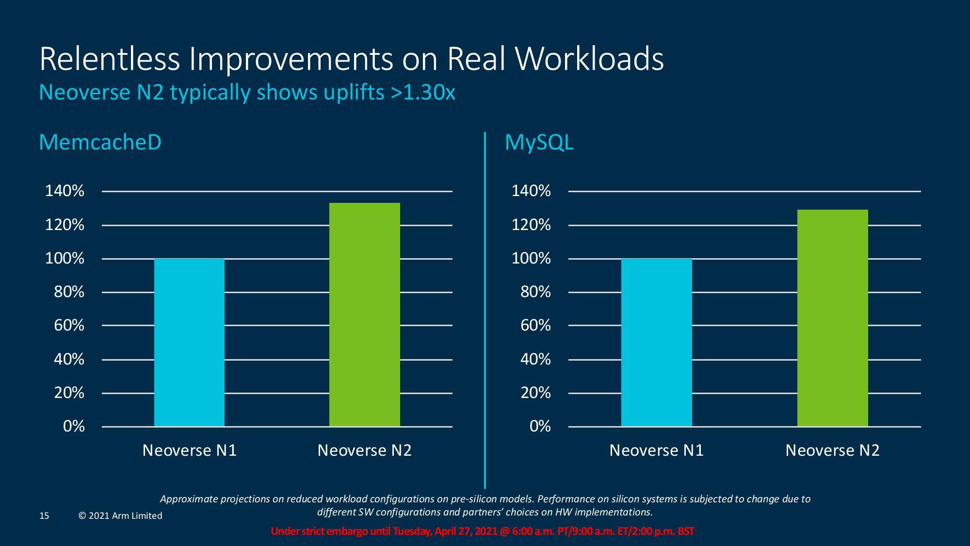
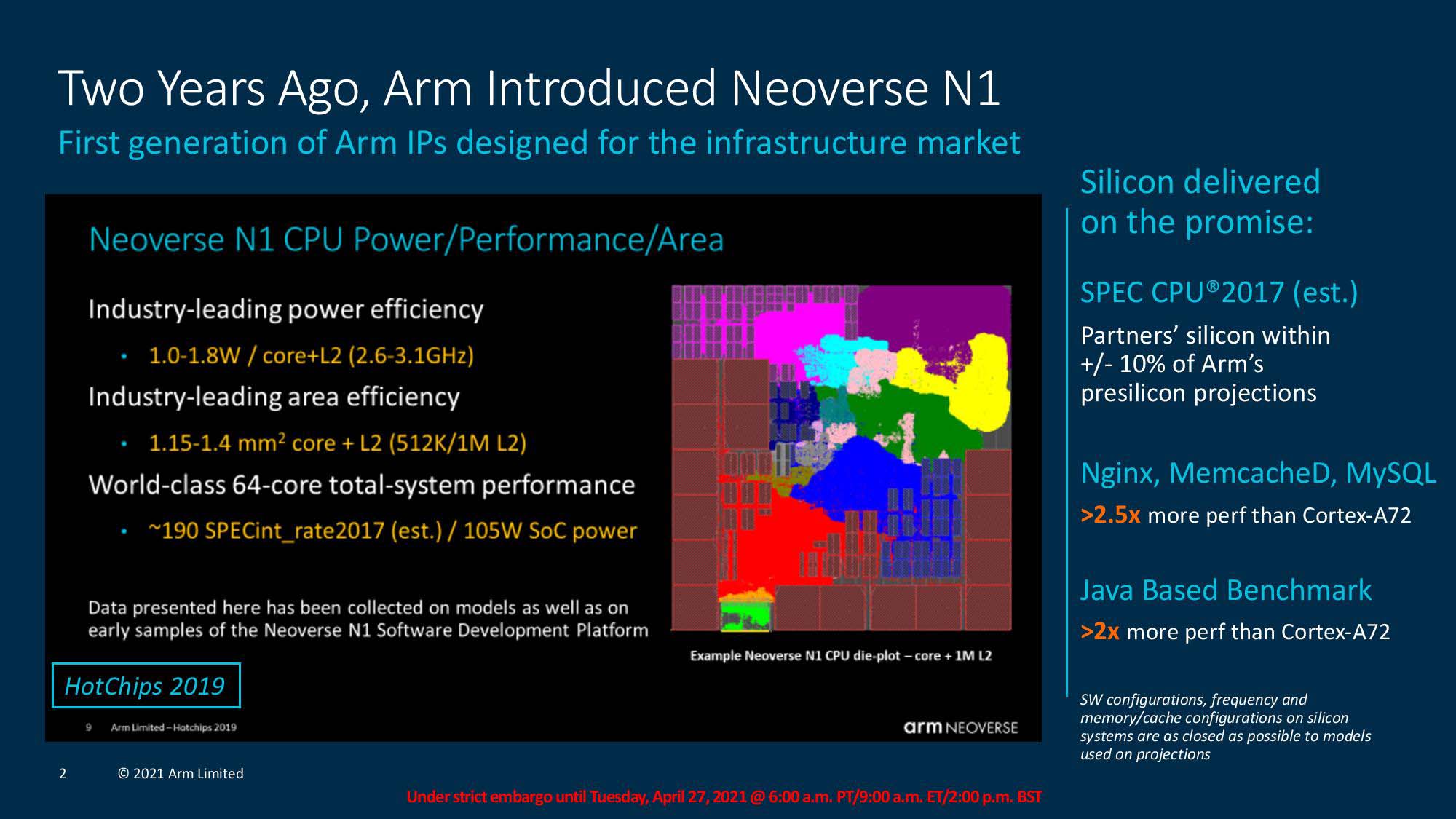
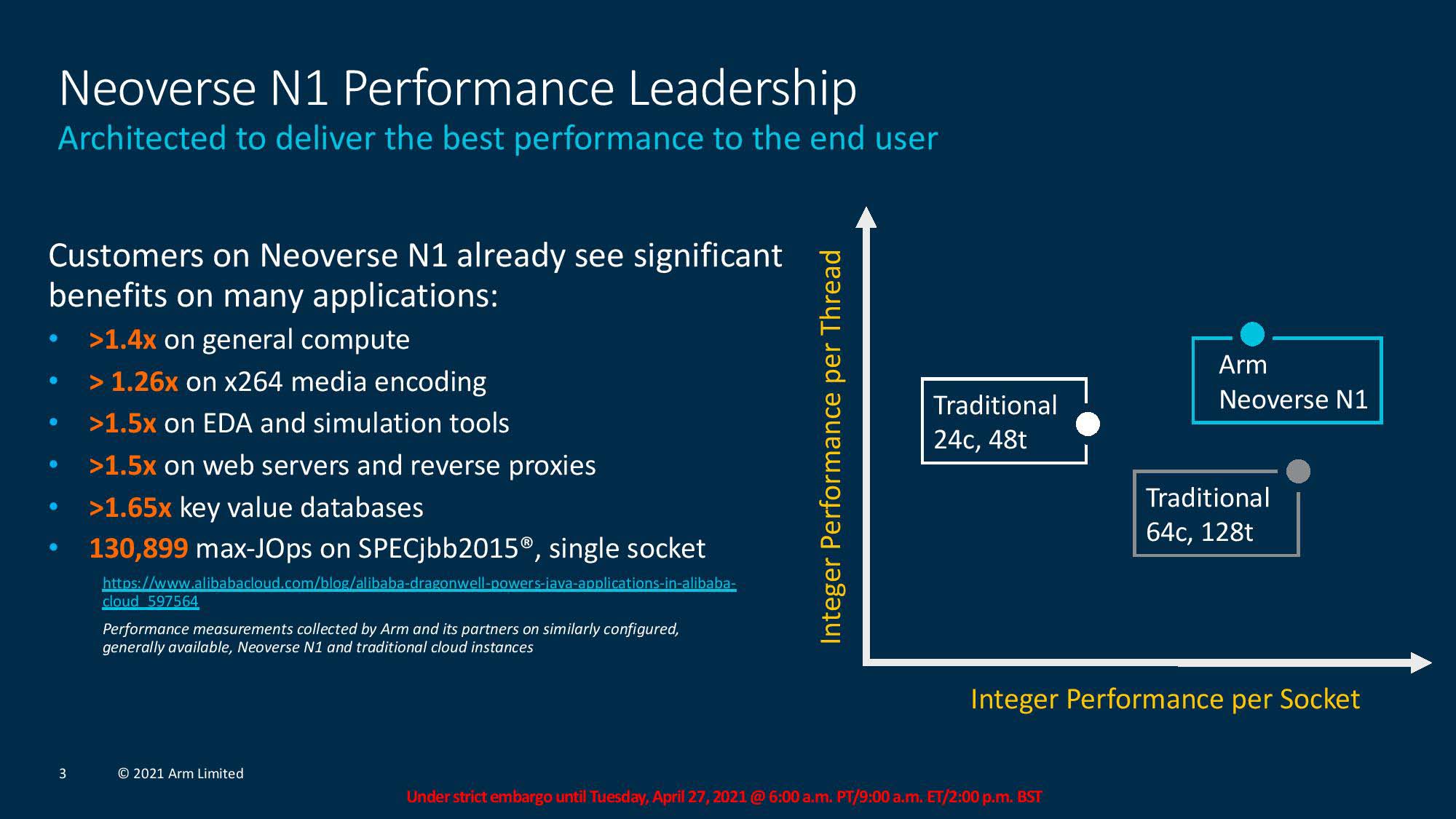
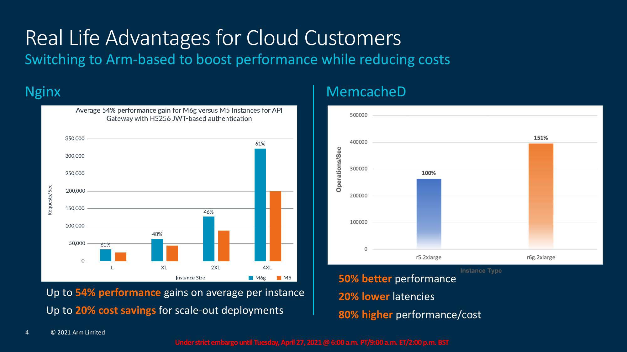
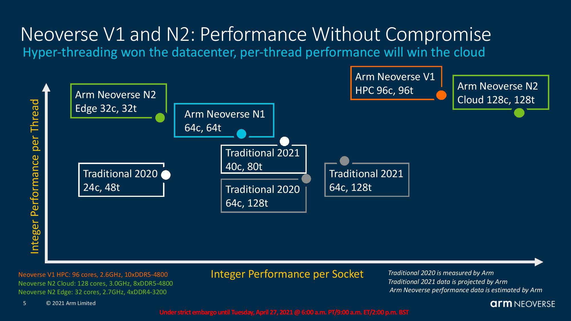
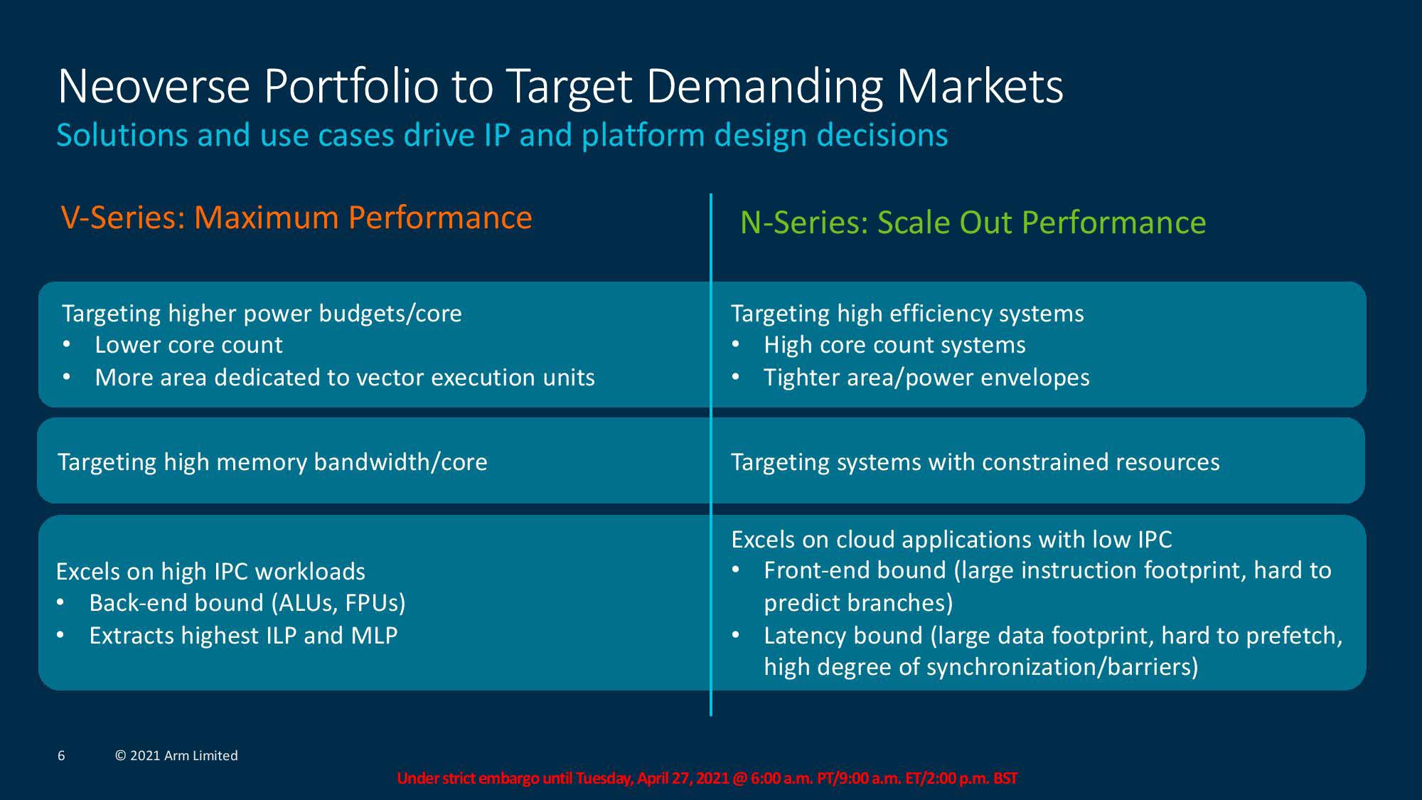
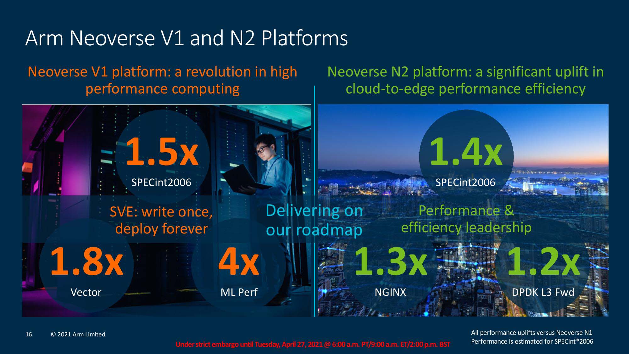
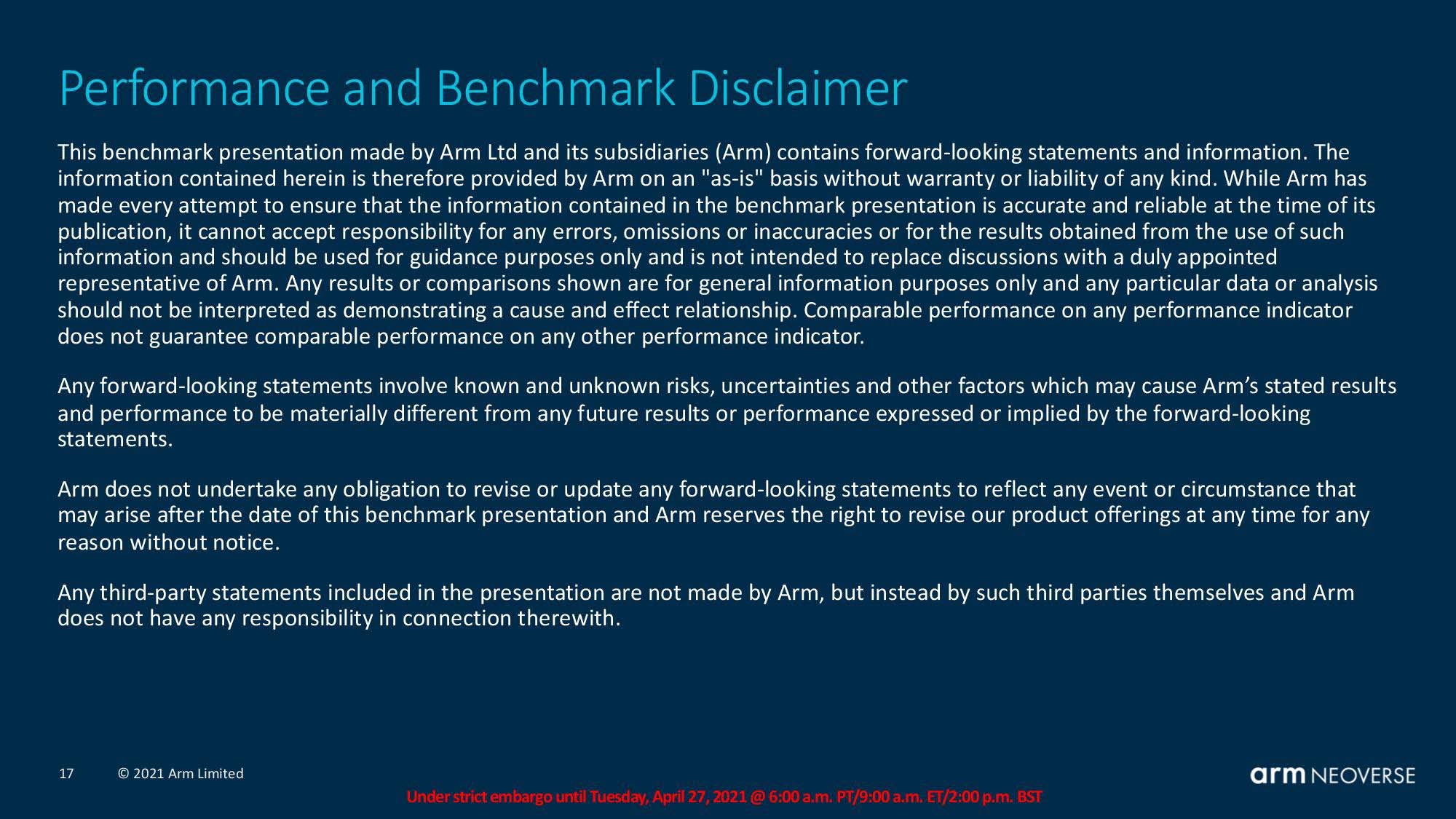
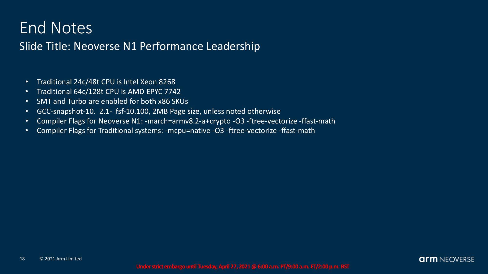
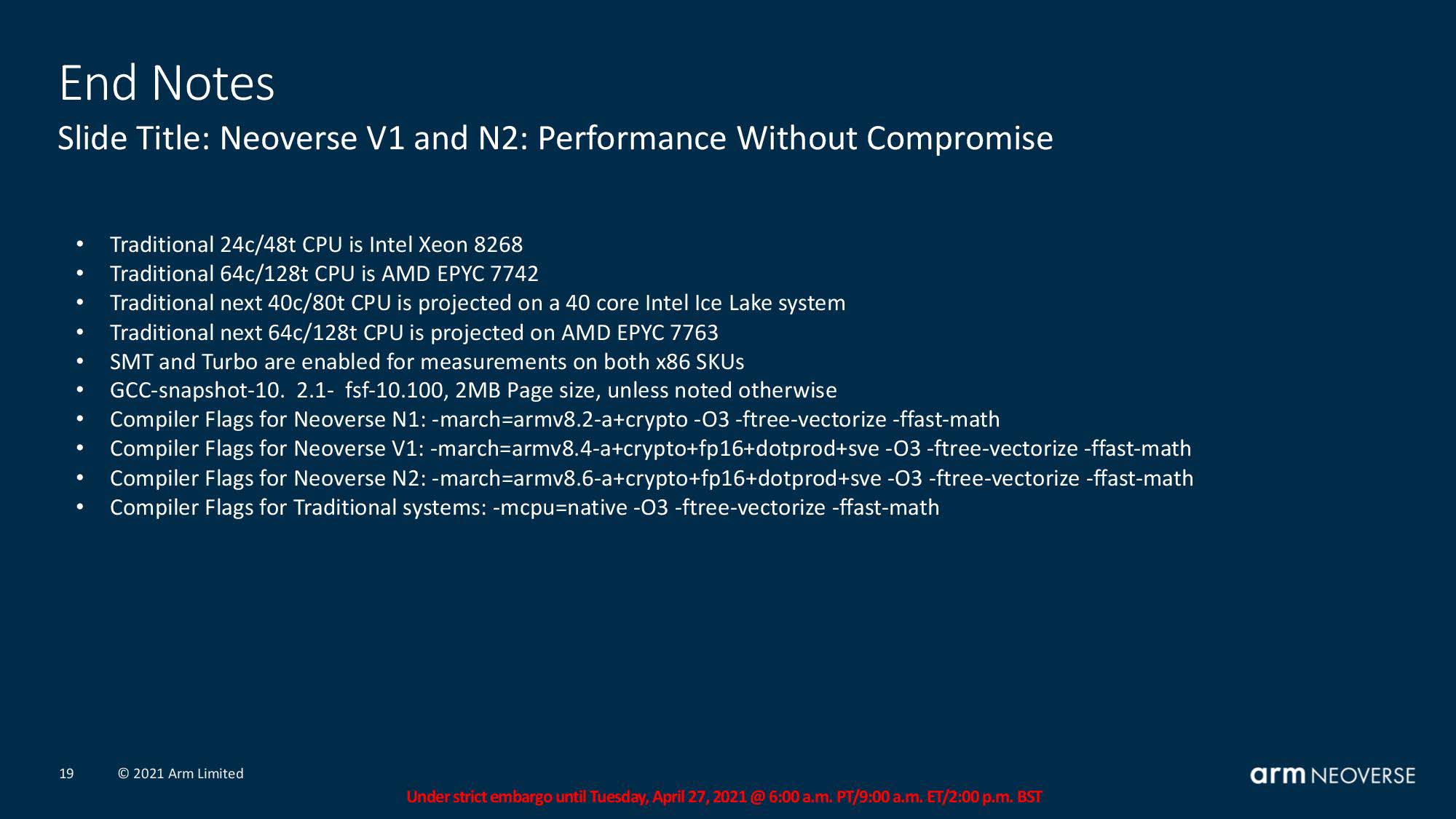
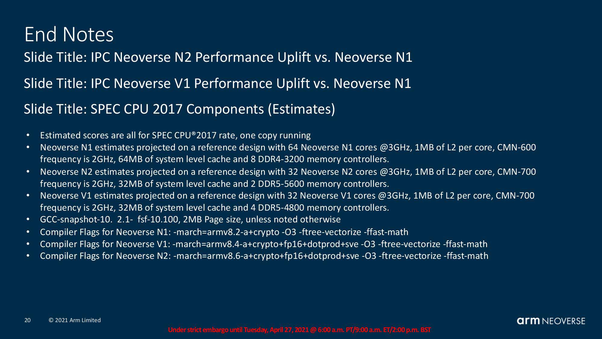
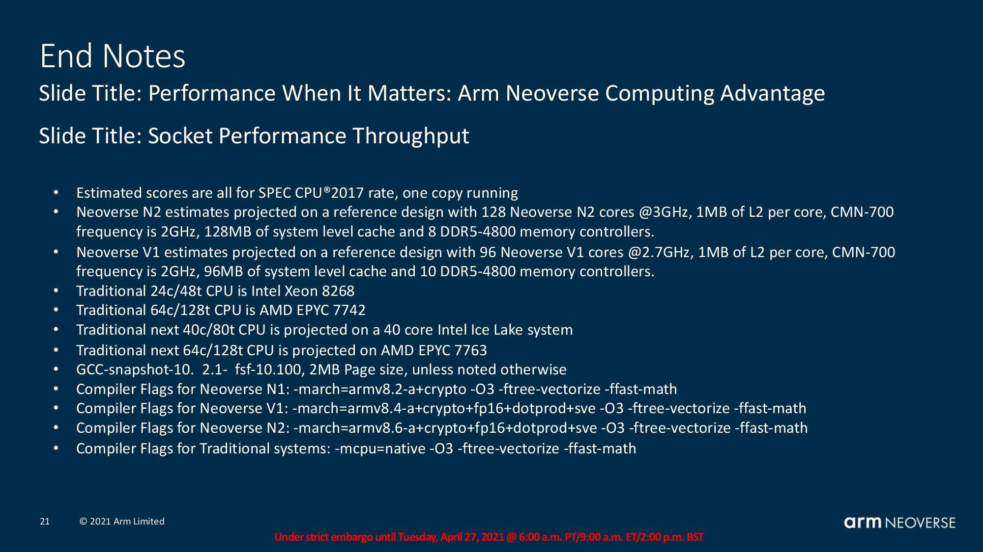
Arm provided the above benchmarks, and as with all vendor-provided benchmarks, you should take them with a grain of salt. We have also included the test notes at the end of the album for further perusal of the test configurations.
Arm's SPEC CPU 2017 single-core tests show a solid progression from N1 to N2, and then a higher jump in performance with the V1 platform. The company also provided a range of comparisons against the Intel Xeon 8268 and an unspecified 40-core Ice Lake Xeon system, and the EPYC Rome 7742 and EPYC Milan 7763.
Coherent Mesh Network (CMN-700)

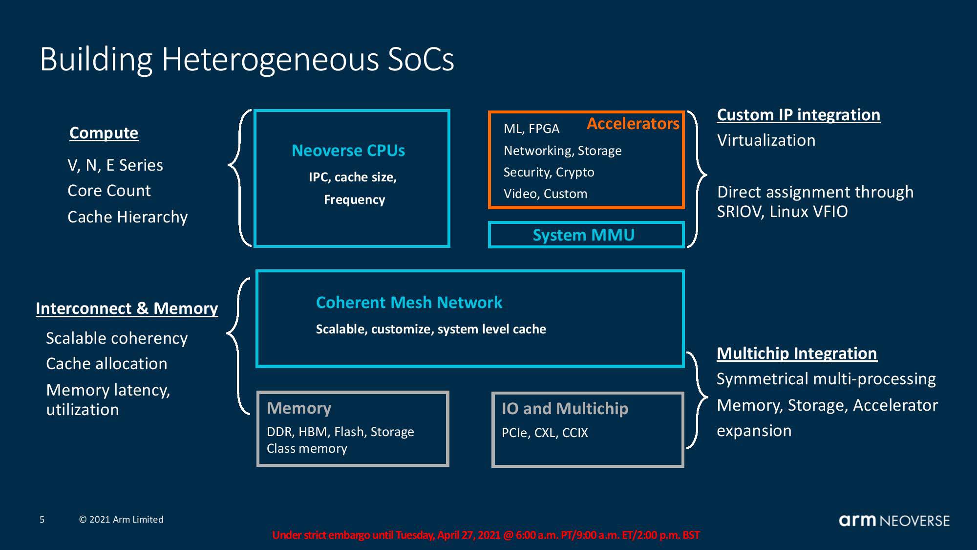
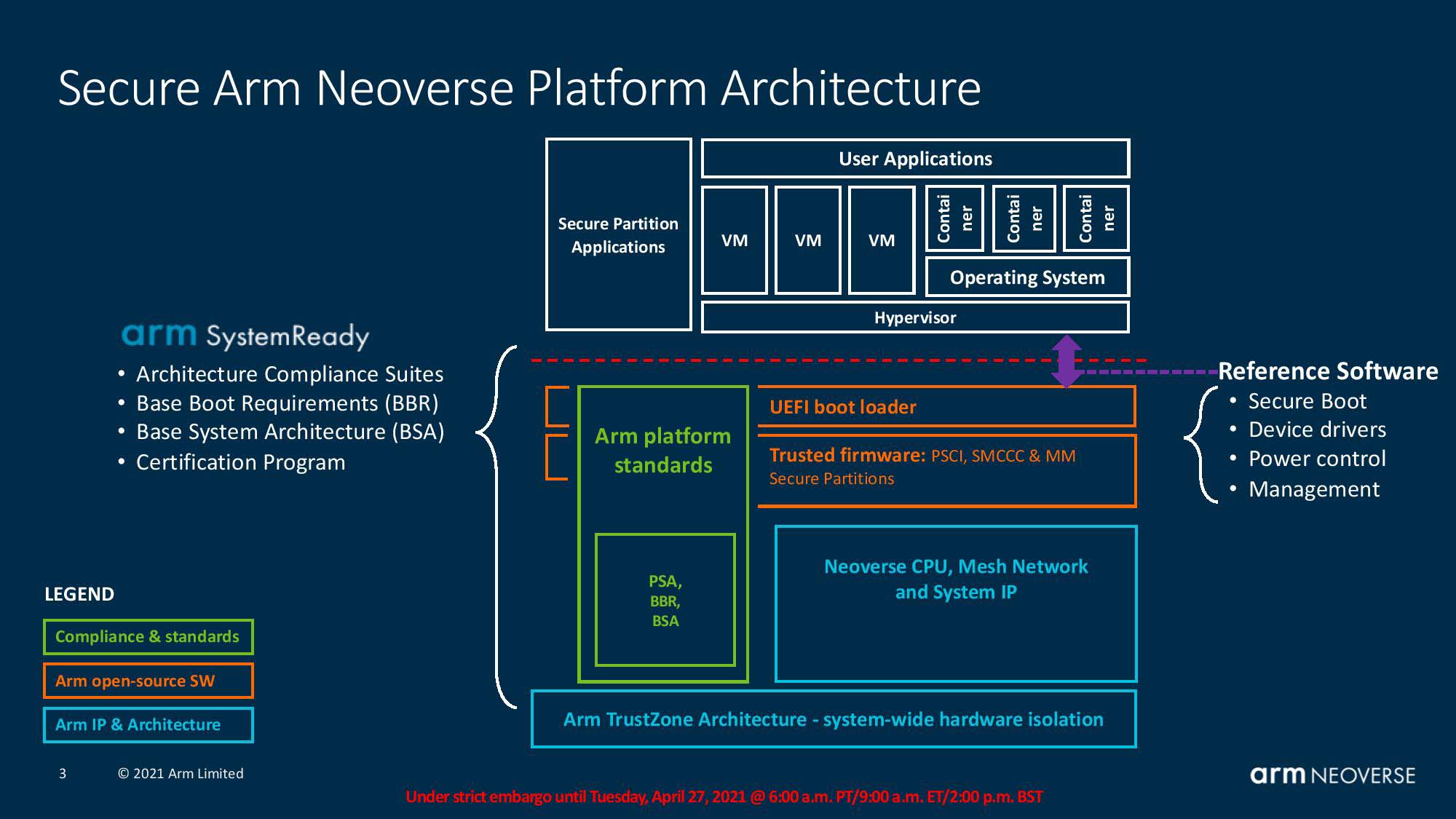
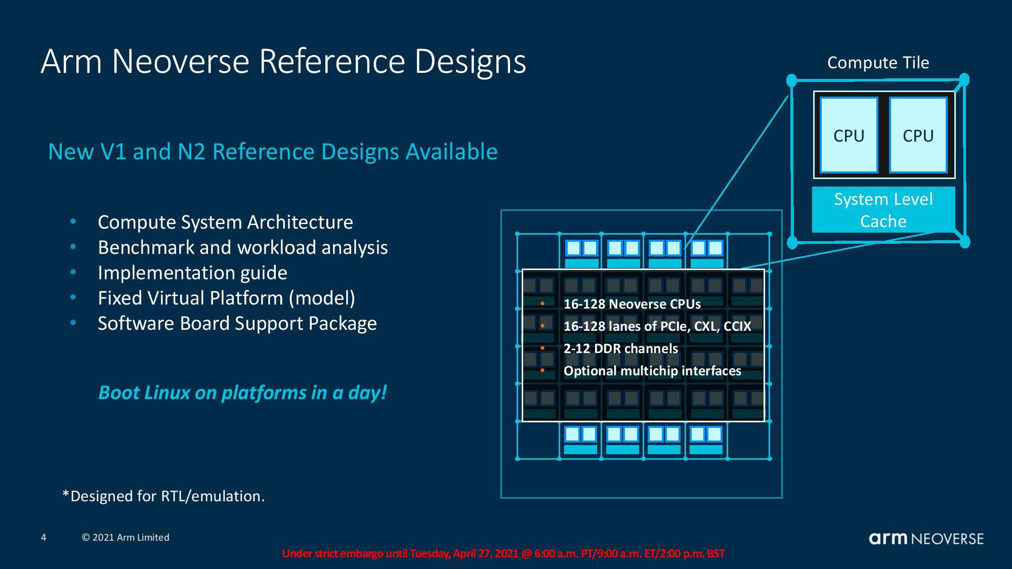
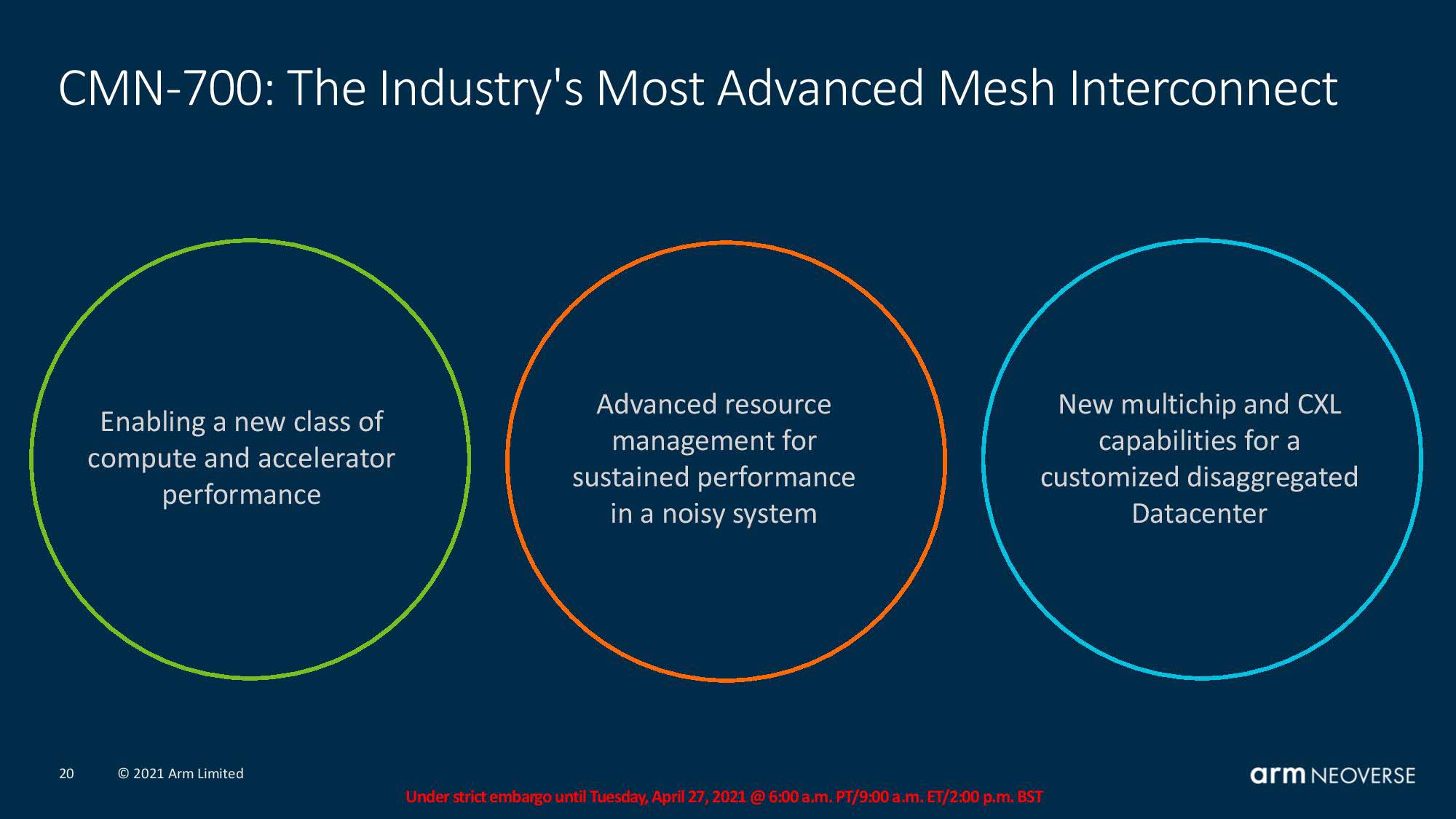
Arm allows its partners to adjust core counts, cache sizes, and use different types of memory, such as DDR5 and HBM and select various interfaces, like PCIe 5.0, CXL, and CCIX, requiring a very flexible underlying design methodology. Add in the fact that Neoverse can span from the cloud and edge to 5G, and the interconnect also has to be able to span a full spectrum of various power points and compute requirements. That's where the Coherent Mesh Network 700 (CMN-700) steps in.
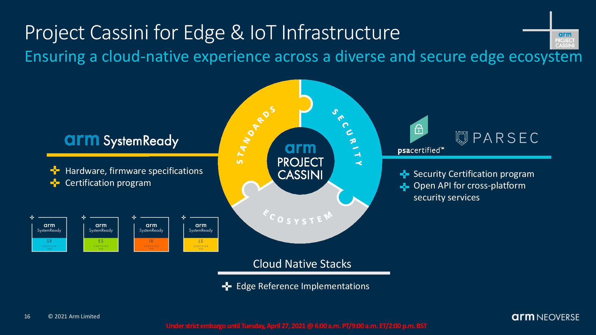
Arm focuses on security through compliance and standards, Arm open-source software, and ARM IP and architecture, all rolled under the SystemReady umbrella that serves as the underpinning of the Neoverse platform architecture.
Arm provides customers with reference designs based on its own internal work, with the designs pre-qualified in emulated benchmarks and workload analysis. Arm also provides a virtual model for software development too.
Customers can then take the reference design, choose between core types (like V-, N- or E-Series) and alter core counts, core frequency targets, cache hierarchy, memory (DDR5, HBM, Flash, Storage Class Memory, etc.), and I/O accommodations, among other factors. Customers also dial in parameters around the system-level cache that can be shared among accelerators.
There's also support for multi-chip integration. This hangs off the coherent mesh network and provides plumbing for I/O connectivity options and multi-chip communication accommodations through interfaces like PCIe, CXL, CCIX, etc.
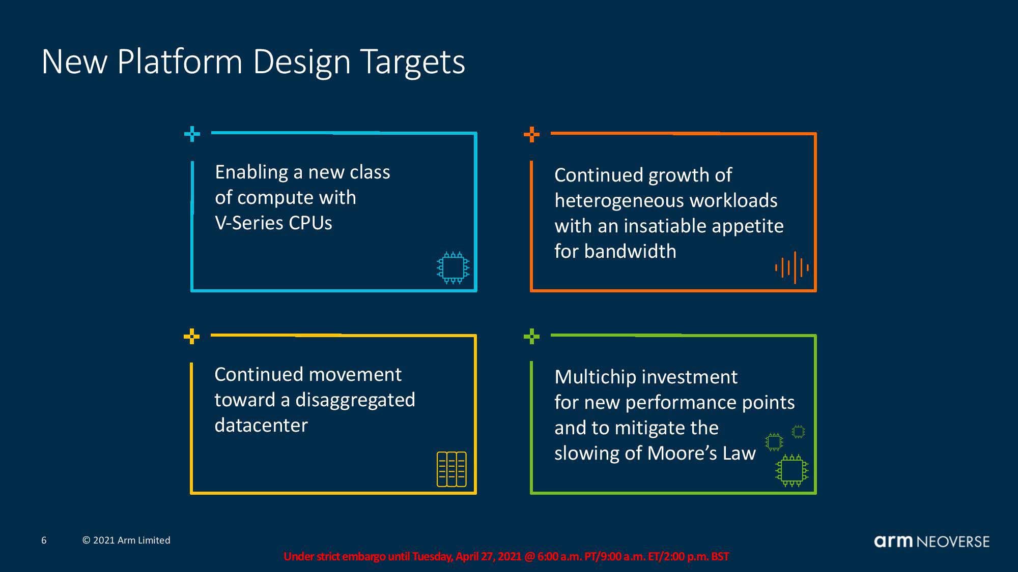
The V-Series CPUs address the growth of heterogeneous workloads by providing enough bandwidth for accelerators, support for disaggregated designs, and also multi-chip architectures that help defray the slowing Moore's Law.
These types of designs help address the fact that the power budget per SoC (and thus thermals) is increasing, and also allow scaling beyond the reticle limits of a single SoC.
Additionally, I/O interfaces aren't scaling well to smaller nodes, so many chipmakers (like AMD) are keeping PHYs on older nodes. That requires robust chip-to-chip connectivity options.
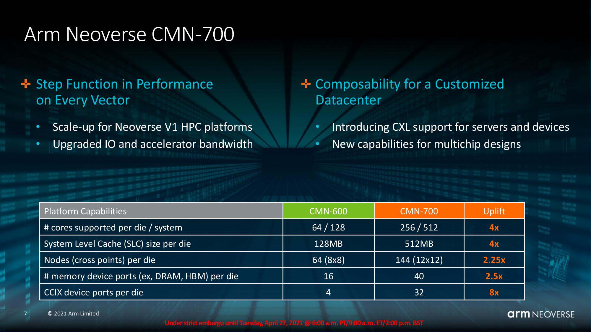
Here we can see the gen-on-gen comparison with the current CMN-600 interface found on the N1 chips. The CMN-700 mesh interface supports four times more cores and system-level cache per die, 2.2x more nodes (cross points) per die, 2.5x memory device ports (like DRAM, HBM) per die, and 8x the number of CCIX device ports per die (up to 32), all of which supplies intense scalability.
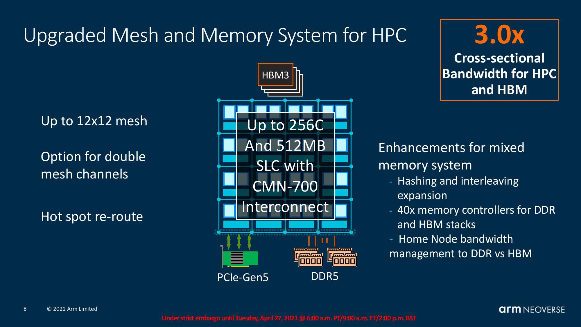
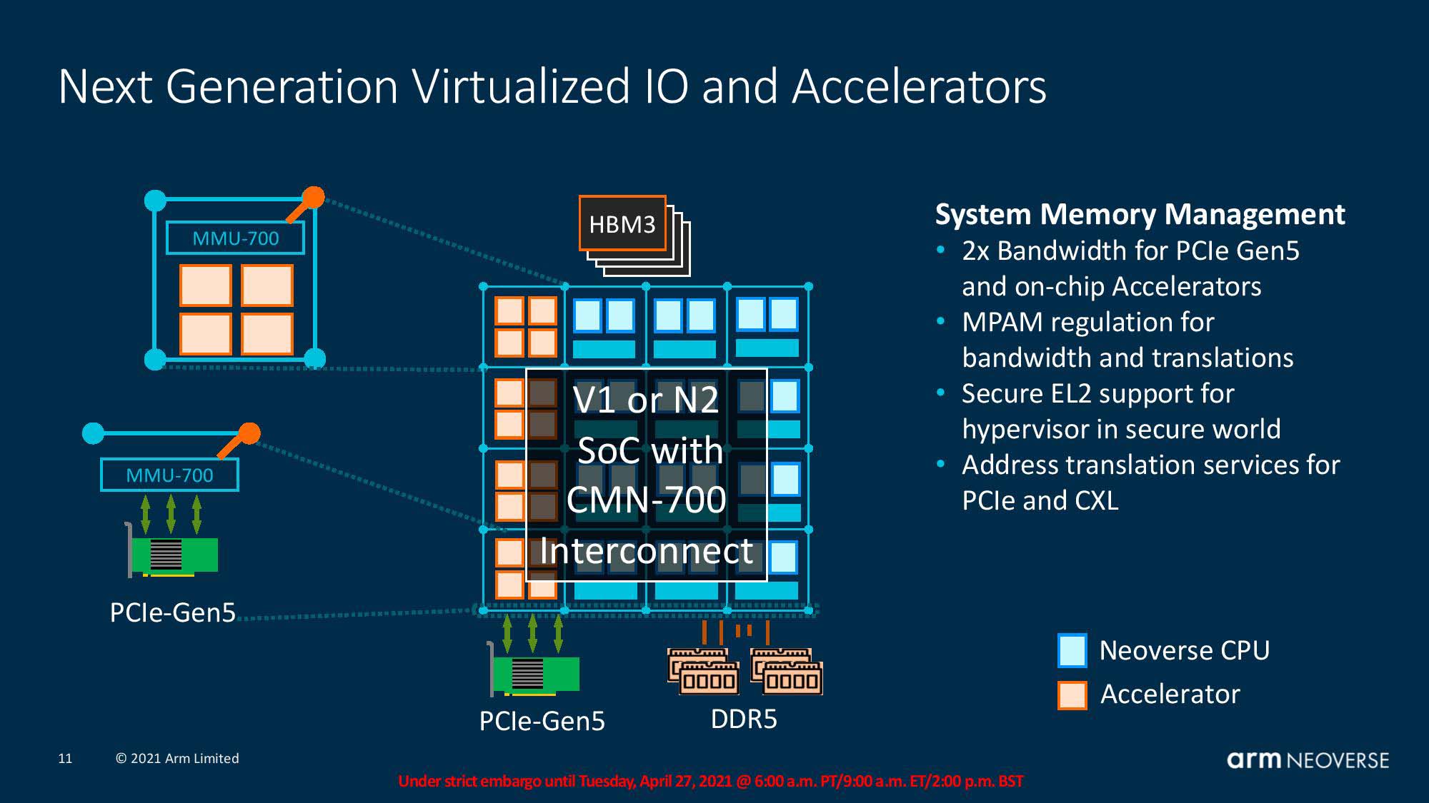
Arm improved cross-sectional bandwidth by 3X, which is important to provide enough bandwidth for scalability of core counts, scaling out with bandwidth-hungry GPUs, and faster memories, like DDR5 and HBM (the design accommodates 40 memory controllers for either/or DDR and HBM). Arm also has options for double mesh channels for increased bandwidth. Additionally, a hot spot reroute feature helps avoid areas of contention on the fabric.
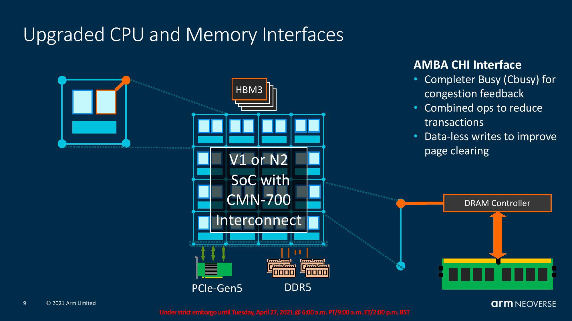
The AMBA Coherent Hub Interface (CHI) serves as the high-performance interconnect for the SoC that connects processors and memory controllers. Arm improved the CHI design and added intelligent heuristics to detect and control congestion, combine operations to reduce transactions, and conduct data-less writes, all of which help reduce traffic on the mesh. These approaches also help with multi-chip scaling.
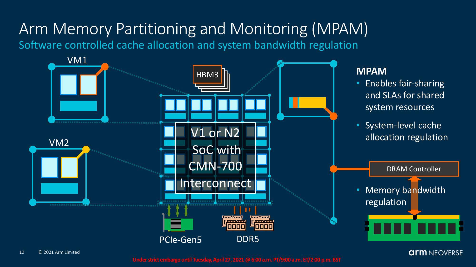
Memory partitioning and monitoring (MPAM) helps reduce the impact of noisy neighbors on system-level cache and isolates VMs to keep them from hogging system level cache (SLC). Arm also extends this software-controlled system to the memory controller as well. All this helps to manage shared resources and reduce contention. The CPU, accelerator, and PCIe interfaces all have to work together as well, so the design applies the same traffic management techniques between those units, too.
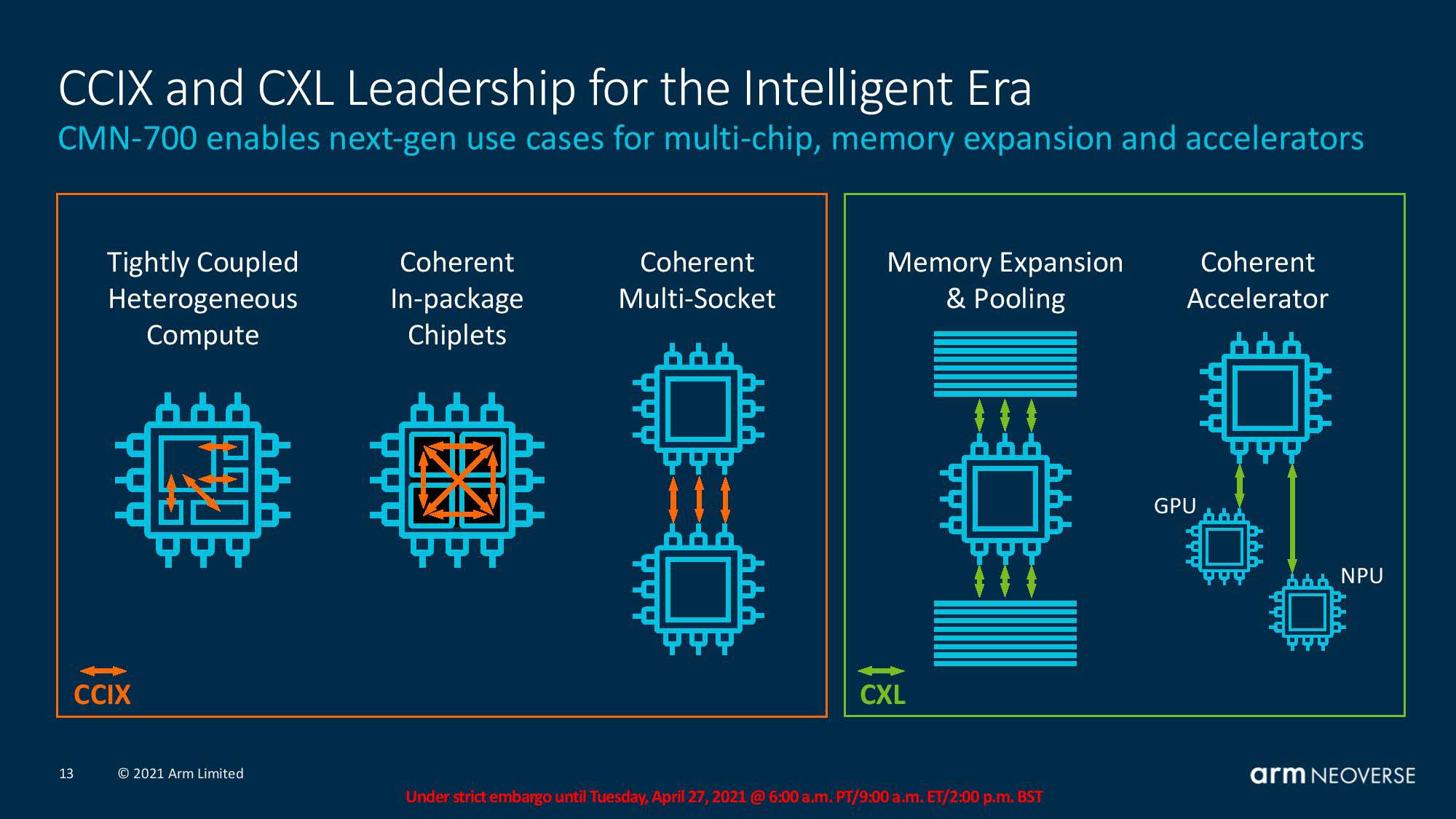
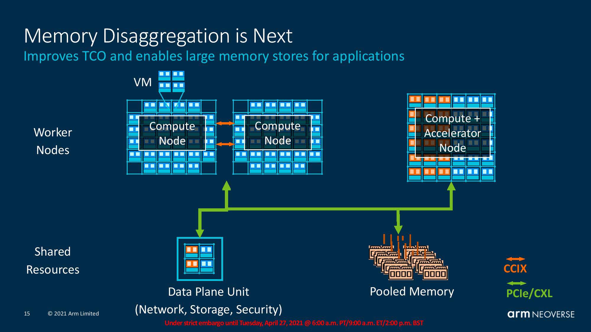
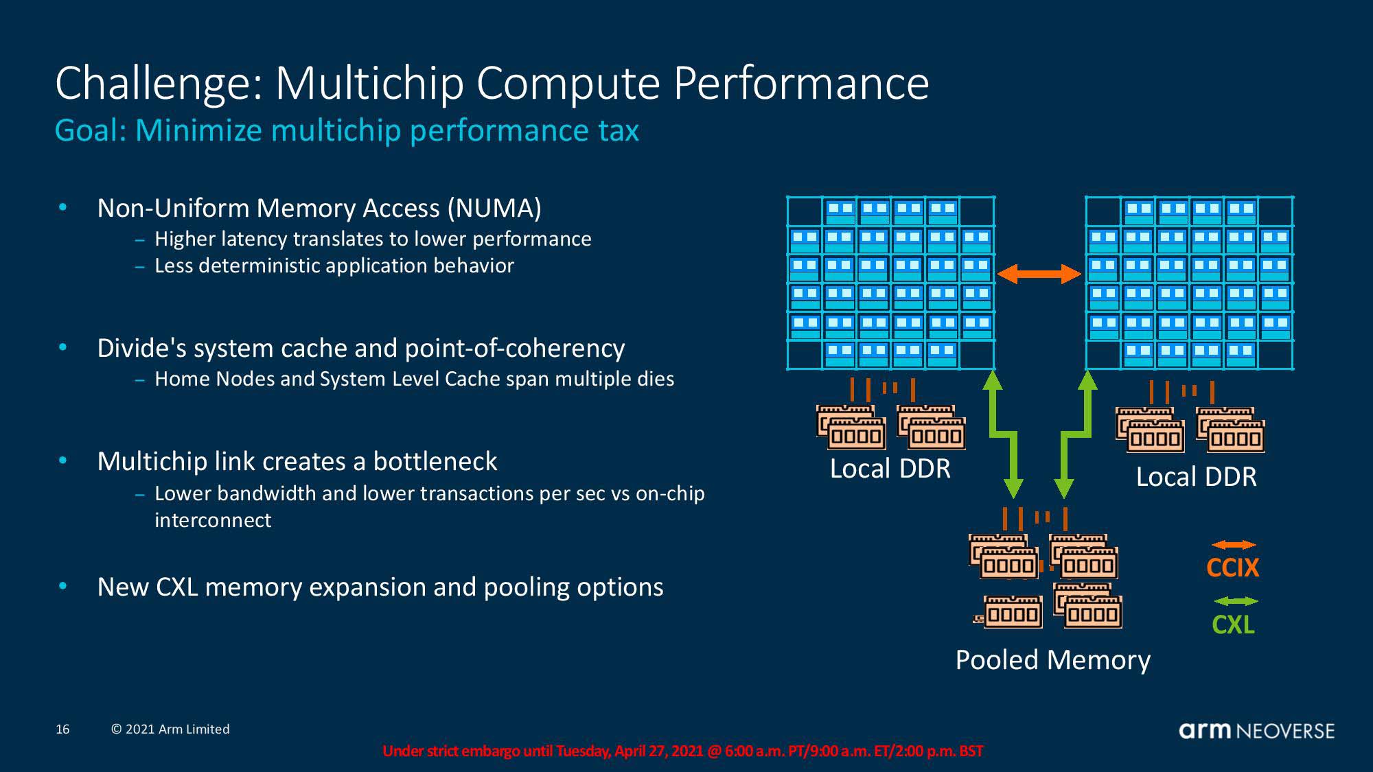
The mesh supports multi-chip designs through CXL or CCIX interfaces, and here we see a few of the use cases. CCIX is typically used inside the box or between the chips, be that heterogenous packages, chiplets, or multi-socket. In contrast, CXL steps in for memory expansion or pools of memory shared by multiple hosts. It's also used for coherent accelerators like GPUs, NPUs, and SmartNICs, etc.
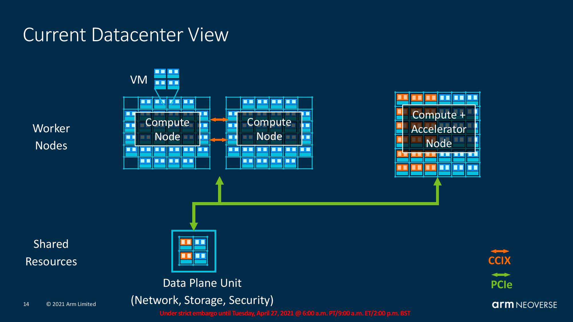
Slide 14 shows an example of a current connection topology — PCIe connects to the DPU (Data Plane Unit - SmartNic), which then provides the interconnection to the compute accelerator node. This allows multiple worker nodes to connect to shared resources.
Slide 15 shows us the next logical expansion of this approach — adding disaggregated memory pools that are shared between worker nodes. Unfortunately, as shown in slide 16, this creates plenty of bottlenecks and introduces other issues, such as spanning the home nodes and system-level cache across multiple dies. Arm has an answer for that, though.
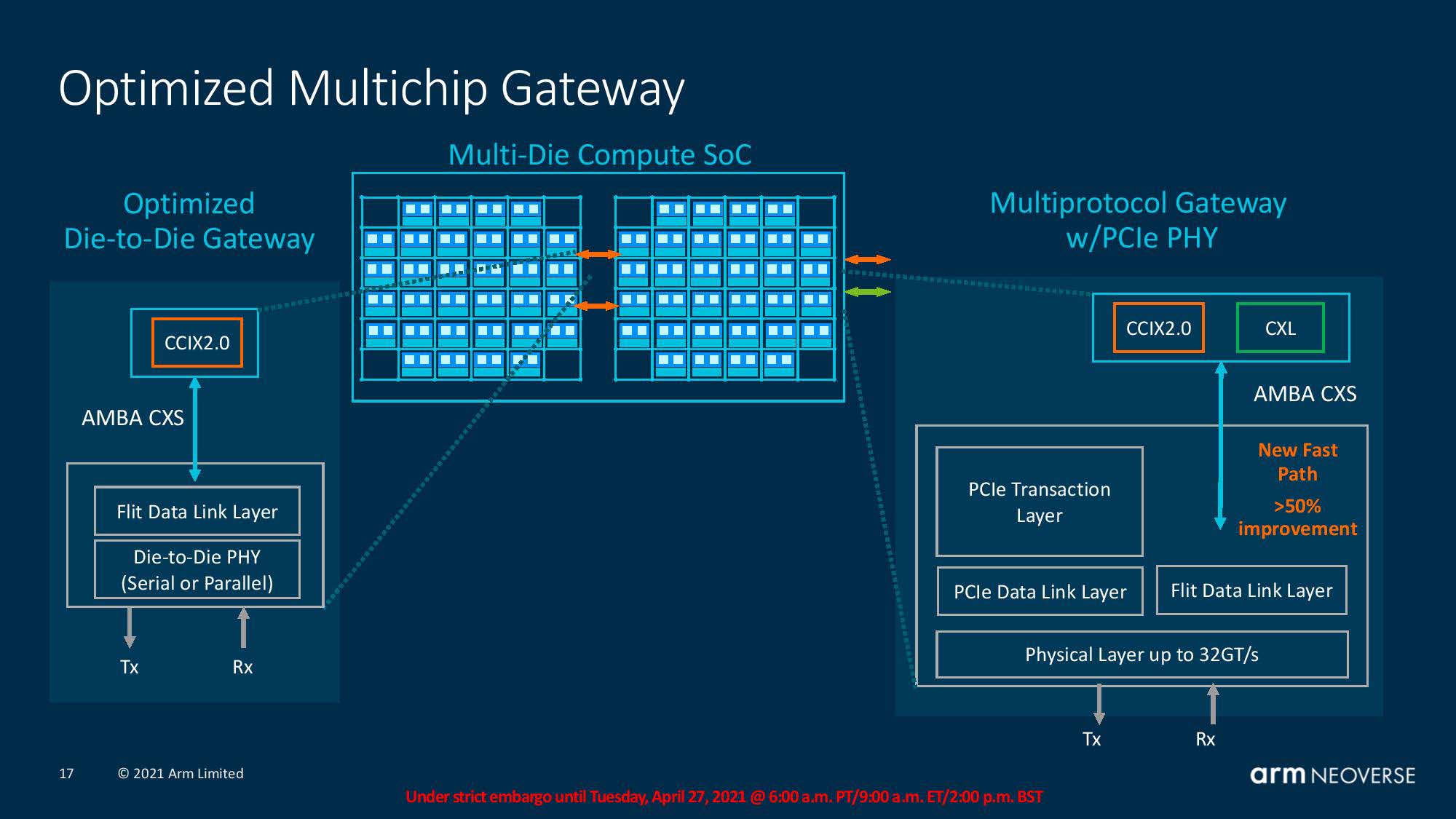
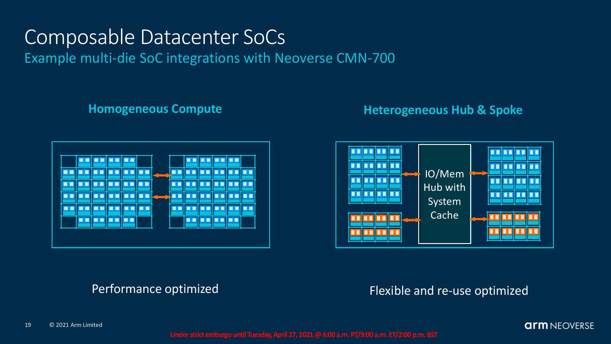
Addressing those bottlenecks requires a re-thinking of the current approaches to sharing resources among worker nodes. Arm designed a multi-protocol gateway with a new AMBA CXS connection to reduce latency. This connection can transport CCIX 2.0 and CXL 2.0 protocols much faster than conventional interconnections. This system also provides the option of using a Flit data link layer that is optimized for the ultimate in low-latency connectivity.
This new design can be tailored for either socket-to-socket or multi-die compute SoCs. As you can see to the left on Slide 17, this multi-protocol gateway can be used either with or without a PCIe PHY. Removing the PCIe PHY creates an optimized die-to-die gateway for lower latency for critical die-to-die connections.
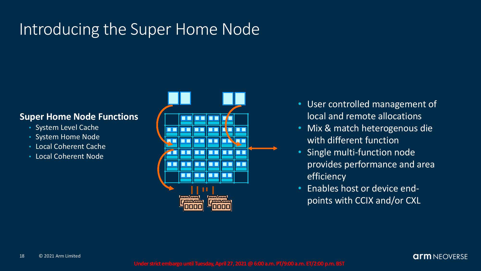
Arm has also devised a new Super Home Node concept to accommodate multi-chip designs. This implementation allows composing the system differently based on whether or not it is a homogenous design (direct connections between dies) or heterogeneous (compute and accelerator chiplets) connected to an I/O hub. The latter design is becoming more attractive because I/O doesn’t scale well to smaller nodes, so using older nodes can save quite a bit of investment and help reduce design complexity.
Thoughts
ARM's plans for a 30%+ gen-on-gen IPC growth rate stretch into the next three iterations of its existing platforms (V1, N2, Poseidon) and will conceivably continue into the future. We haven't seen gen-on-gen gains in that range from Intel in recent history, and while AMD notched large gains with the first two Zen iterations, as we've seen with the EPYC Milan chips, it might not be able to execute such large generational leaps in the future.
If ARM's projections play out in the real world, that puts the company not only on an intercept course with x86 (it's arguably already there in some aspects), but on a path to performance superiority.
Wrapping in the amazingly well-thought-out coherent mesh design makes these designs all the more formidable, especially in light of the ongoing shift to offloading key workloads to compute accelerators of various flavors. Additionally, bringing complex designs, like chiplet, multi-die, and hub and spoke designs all under one umbrella of pre-qualified reference designs could help spur a hastened migration to Arm architectures, at least for the cloud players. That attraction of licensable interconnections that democratize these complex interfaces is definitely yet another arrow in Arm's quiver.
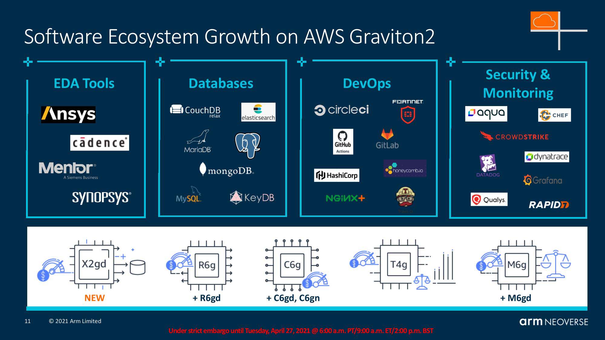
Perhaps one of the most surprising tidbits of info that Arm shared in its presentations was one of the smallest — a third-party firm has measured that more than half of AWS's newly-deployed instances run on Graviton 2 processors. Additionally, Graviton 2-powered instances are now available in 70 out of the 77 AWS regions. It's natural to assume that those instances will soon have a newer N2 or V1 architecture under the hood.
This type of uptake, and the economies of scale and other savings AWS enjoys from using its own processors, will force other cloud giants to adapt with their own designs in kind, perhaps touching off the type of battle for superiority that can change the entire shape of the data center for years to come. There simply isn't another vendor more well-positioned to compete in a world where the hyperscalers and cloud giants battle it out with custom silicon than Arm.

Paul Alcorn is the Editor-in-Chief for Tom's Hardware US. He also writes news and reviews on CPUs, storage, and enterprise hardware.
-
ginthegit Soooooo! Let me get this right, rather than ARM keeping true to their Usual RISC formula of hardwairing all this complexity, they are now adding to the Instructions that access the cores. That would mean that the Kernel (like in windows) now has control of how the CPU routing is organised and brings all the overheads and latency with it.Reply
The RISC architectures were ment to be Hardware Driven and routed so that its concepts didn't need to add to the Basic ISA. With these changes we are adding to the ISA to access certain elements of the core meaning that is is becoming CISC by definition.
So, in other words, the new management running ARM are now cutting the corners of the rules. Or their Engineers are not good enough to create the Sequential logic control to reroute this functionality as Native (true RISC).
The Mesh design could have been made as a round robin style core based PIPELINE, where each core is controlled by a central core (like with the old Cell architecture) and Pipeline the instructions to various cores, then collecting the response from the other end. There problem thus becomes that the traditional PIPELINE model would become massively more complex. You can only have one or the other. Only when they decide to restructure the ISA and reduce the amount of clock cycles per instruction, will they ever be able to reduce the latency, to effectively be able to make a Multicore work effectively as a co processor. Current ISA takes 4-6 steps to pass through a Instruction decode, and more steps on the accumulator to complete and free up the accumulator for next instruction. But SMT or its equivalent would need to be removed.