SK Hynix Demos 24GB HBM3 at 6.4 Gbps and Samsung Works on Cheaper H-Cube
HBM is developing, just not for consumers.
It's unlikely high-bandwidth memory (HBM) will replace conventional types of DRAM any time soon, but the ongoing evolution of the HBM ecosystem will both make usage of such memory cheaper and will enable even more sophisticated HBM installations. This week SK Hynix demonstrated its 24GB HBM3 memory stacks for bandwidth-hungry system-on-chips (SoCs), and Samsung introduced its H-Cube technology that promises to democratize usage of HBM for accelerators.
24GB in a Single Chip
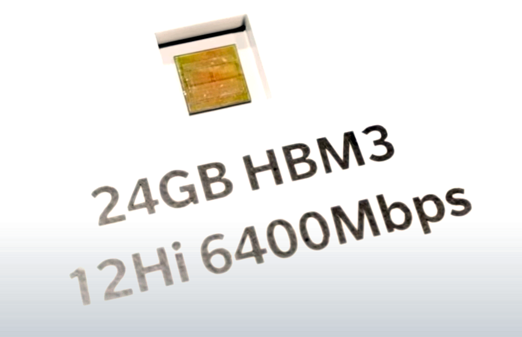
SK Hynix said that it had developed its 12-Hi 24GB HBM3-6400 memory stacks comprised of 12 DRAM devices interconnected using through silicon vias (TSVs) and placed on a base die less than a month ago. IP companies already offer HBM3 controllers and PHY, and there are a number of upcoming SoCs that will use HBM3 memory, but none of them are ready to be showcased. So, SK Hynix decided to show the actual 24GB memory chips with a 6.4 GT/s data transfer rate and a 1024-bit interface that can provide a bandwidth of up to 819 GB/s, as noticed by ServeTheHome at the OCP Summit.
The demonstration is an indicator that SK Hynix at least has HBM3 samples and can demonstrate them outside of the lab. Still, for obvious reasons SK Hynix cannot disclose names of its SoC partners that plan to use these memory stacks first. Meanwhile, given that bandwidth-hungry chips tend to serve enterprise or high-performance computing (HPC) applications, we can be sure that the first SoCs to use HBM3 will be quite expensive.
Samsung H-Cube
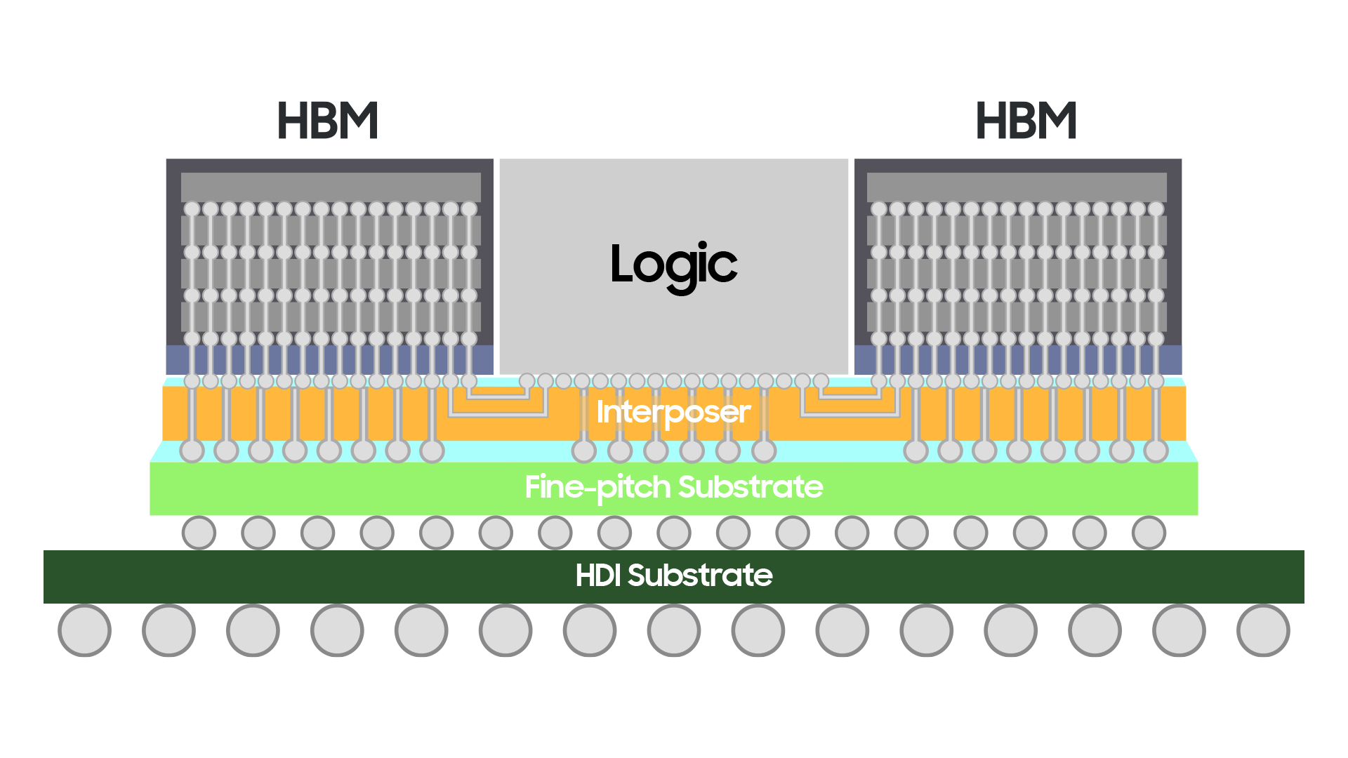
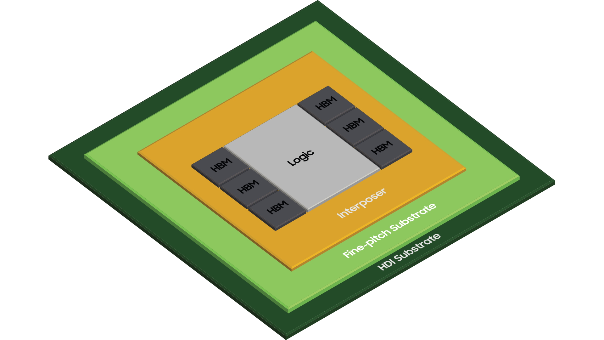
Speaking of HBM costs, there are several reasons why HBM-equipped solutions are expensive. Firstly, building high-capacity memory chips is pricey and stacking many of them together on a base die makes such known good stacked dies (KGSDs) precious. Secondly, connecting these KGSDs to an SoC using a substrate is costly too, as substrates tend to get prohibitively large and expensive with the increase in the number of memory stacks used. This is where Samsung's and Amkor's new Hybrid-Substrate Cube (H-Cube) technology comes into play, as it promises to make packages with six or more HBM stacks cheaper.
Normally, interposers are placed on fine-pitch substrates (that tend to be larger than interposers and also very expensive) that are than installed onto motherboards. Samsung's H-Cube technology applies a relatively large hybrid High-Density Interconnection (HDI) substrate that sits between the fine-pitch substrate (FPS) and the motherboard. Since the FPS no longer has to be large enough to be placed directly onto the motherboard, its solder ball pitches can be decreased by 35%. Samsung says that its H-Cube technology ensures stable power supply and minimizes the signal loss or distortion when stacking multiple logic chips and HBMs.
Samsung stresses that its H-Cube technology works best with higher-end HBM implementations with six or more memory chips. Yet, nothing stops anyone from using it for more entry-level products.
Both HBM3 and H-Cube should help to improve the bandwidth and adoption of HBM technologies going forward. Will we see another consumer product using HBM, like AMD's R9 Fury and RX Vega families? Probably, though it may not happen for another generation or two of GPUs.
Get Tom's Hardware's best news and in-depth reviews, straight to your inbox.

Anton Shilov is a contributing writer at Tom’s Hardware. Over the past couple of decades, he has covered everything from CPUs and GPUs to supercomputers and from modern process technologies and latest fab tools to high-tech industry trends.


