Into the GPU Chiplet Era: An Interview With AMD's Sam Naffziger
A look into the future RDNA 3 architecture
We recently had a chance to speak with Sam Naffziger, AMD’s Senior Vice President, Corporate Fellow, and Product Technology Architect, about what's been happening with Radeon graphics over the past several years and what we can expect going forward. AMD recently provided some tantalizing details on its upcoming RDNA 3 GPU architecture, which is slated to launch before the end of the year with a chiplet-based design, and that provides the background for our interview and Q&A session. We've taken our discussion and distilled it down to the key points, so we won't present this in interview format.
Naffziger has been at AMD for 16 years and is responsible for multiple product areas, with a focus on driving higher performance per watt and improving the overall competitiveness of AMD's CPUs and GPUs. He's also one of the primary people behind AMD's chiplet architecture, which has proven incredibly successful in the Ryzen and EPYC CPU lines and will now come in some form to AMD RDNA 3 graphics. Naffziger outlined the challenges facing the company and how he feels that innovative tech, like a chiplet-based GPU architecture, can result in both improved performance and power efficiency.
Running Into the Power Wall
At the heart of modern microprocessor design, power use and efficiency are becoming increasingly problematic, and no company is immune to the side effects. All signs point to increased power consumption from next-gen GPUs: The PCIe 5.0 power interface and upcoming power supplies that support it can supply up to 600W over a single 16-pin connector, portending a broader industry shift to higher-power GPUs. It's basically known that Nvidia's Ada architecture will push to higher power limits than we've seen in the past — current rumors suggest we might see 450W TBP (typical board power) and perhaps even as much as 600W TBP for the top RTX 40-series GPUs. There hasn’t been word yet of TBP’s for AMD’s RDNA 3, but it’s fair to think they could follow the same trend.
So while our conversation focused on AMD’s approach to improving efficiency, the question of overall power consumption remains. Naffziger confirmed that we could expect total power consumption to increase in next-gen GPUs, but explained how focusing on efficiency can maximize performance.
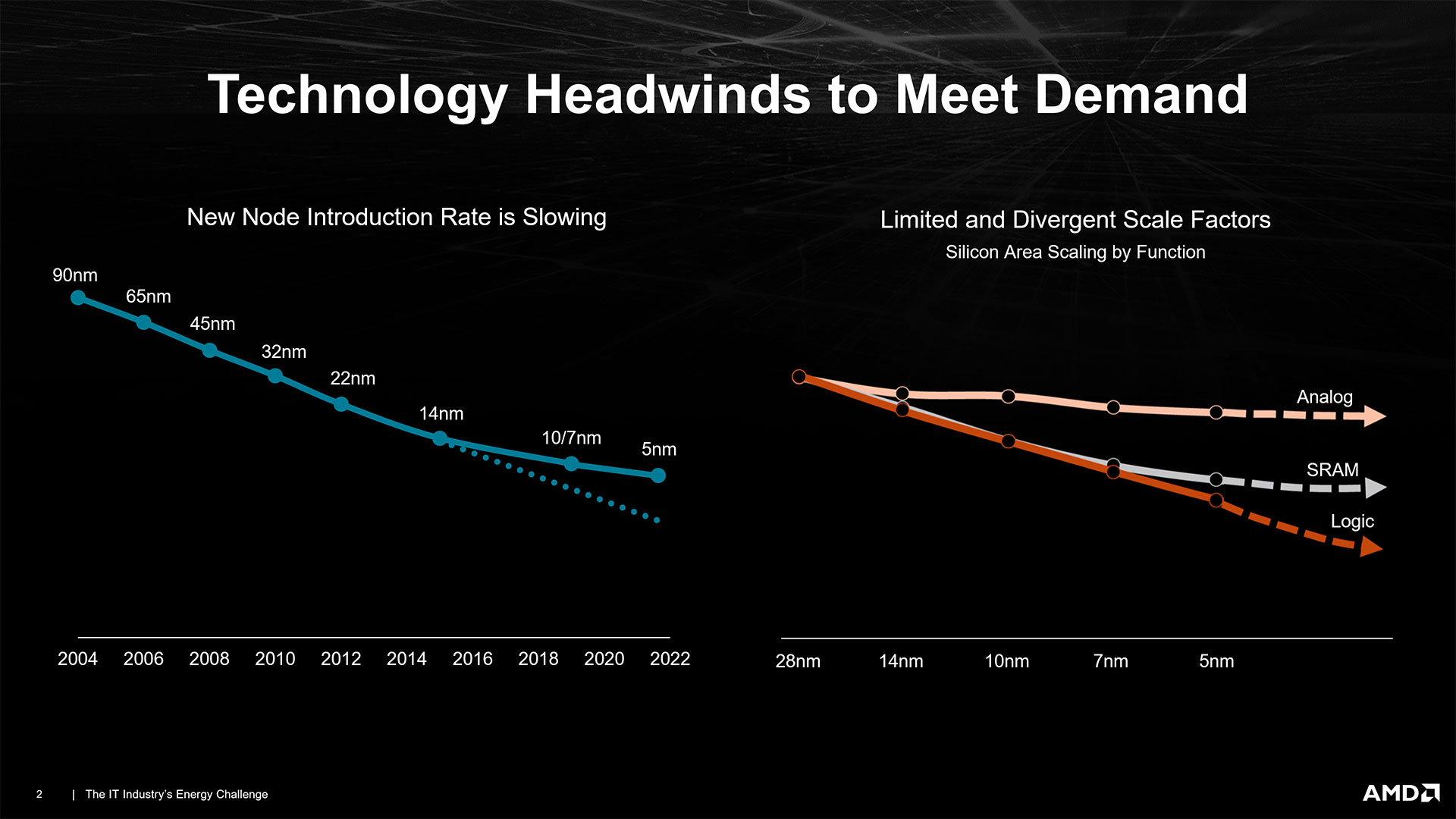
“It's really the fundamentals of physics that are driving this,” Naffziger explained. "The demand for gaming and compute performance is, if anything, just accelerating, and at the same time, the underlying process technology is slowing down pretty dramatically — and the improvement rate. So the power levels are just going to keep going up. Now, we've got a multi-year roadmap of very significant efficiency improvements to offset that curve, but the trend is there.”
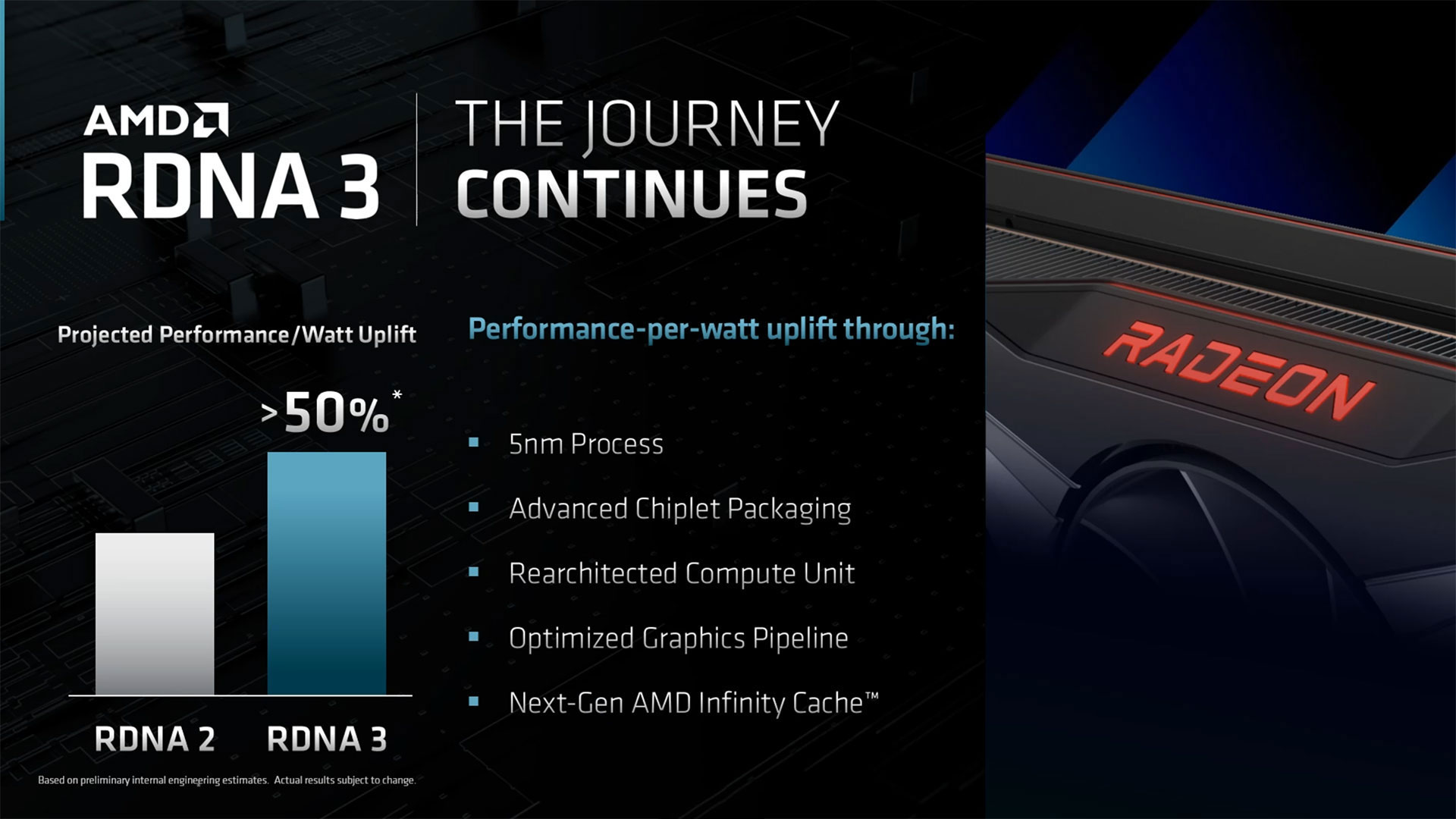
AMD claims a 50% improvement in performance per watt for both RDNA and RDNA 2, and that it's targeting another 50% improvement in performance per watt with RDNA 3. That can mean a lot of different things: 50% more performance at the same power, the same performance while using 33% less power, or somewhere else along the performance and power curve. Also note that, like Nvidia and Intel, AMD only needs to have one particular scenario where it can say performance per watt improved by 50% to claim such gains.
Naffziger explained some of the improvements AMD has seen with its previous RDNA 2 architecture. For example, if it can run at 2.5 GHz and 1.0V instead of 1.2V, the latter would require 40% more power. By leveraging expertise from its CPU design teams, Naffziger said that AMD has been able to drive higher clocks with RDNA 3 while remaining efficient. AMD has long discussed its strategy of ‘cross-pollinating’ CPU and GPU design teams, bringing the best tech from both sides of the house to each new CPU and GPU design. Naffziger said that the current GPU cores are "intrinsically more power efficient," but a business decision still needs to be made.
"Performance is king," stated Naffziger, "but even if our designs are more power-efficient, that doesn't mean you don't push power levels up if the competition is doing the same thing. It's just that they'll have to push them a lot higher than we will."
In other words, don't be surprised if AMD, similar to Nvidia, ends up increasing TBPs for its top RDNA 3 graphics cards.
Get Tom's Hardware's best news and in-depth reviews, straight to your inbox.
Power Efficiency and Performance per Watt
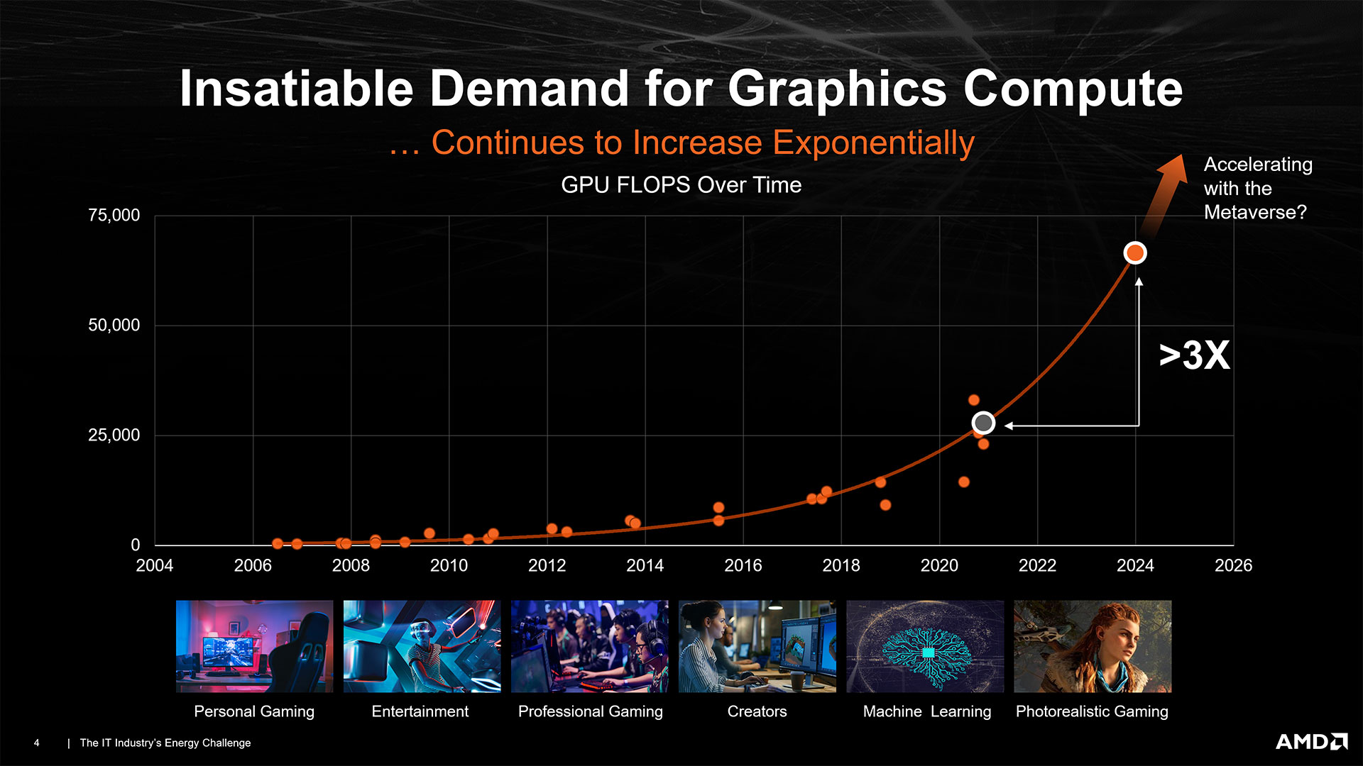
The fundamental challenges of a slowing rate of improvement from Moore’s Law have to be offset with clever engineering and a focus on power efficiency, and AMD has proven itself in this realm. Right now, AMD's Zen 3 CPUs generally lead Intel when it comes to efficiency and performance per watt, though we'll have to see how that changes with Zen 4 and Ryzen 7000. In addition, AMD's RDNA 2 GPUs also tend to beat rival Nvidia's GPUs in efficiency, depending on the specific models you compare. This is critical as we've seen a rapid escalation to higher power CPUs and GPUs in recent years, leading to more heat and expensive cooling solutions.
Looking specifically at AMD's graphics parts over the past two generations, RDNA back in 2019 delivered a clear 50% or more improvement in performance per watt compared to the previous generation Vega and Polaris architectures. For example, our own testing results from our GPU benchmarks hierarchy show that the RX 5700 XT averaged 74 fps in our 1080p test suite while consuming 214W, compared to 57 fps from the RX Vega 64 that consumed 298W — that's actually an 80% boost in performance per watt with those two parts.
RDNA 2 in 2020 was able to again deliver up to 50% higher performance per watt compared to RDNA. Except, we have to clarify that "up to" business. For example, the RX 6600 averaged 67 fps at 1080p ultra and consumed 137W, which is 41% better efficiency than the RX 5700 XT. Meanwhile, the RX 6700 XT delivered 96 fps while using 215W, only a 30% improvement in pure efficiency, while the RX 6800 XT reached 124 fps and used 303W, only 18% better efficiency. The RX 5500 XT 8GB, however, averaged 40 fps with 126W, so the RX 6600 was 54% more efficient in at least some cases — and that's using a similar 128-bit memory interface.
More impressively, these gains all came without a change in process node, as both RDNA and RDNA 2 used TSMC's 7nm N7 tech (though some of the more recent GPUs like Navi 24 now use N6).
AMD announced at its financial analyst day that it's again committed to a 50% improvement in performance per watt with RDNA 3, leveraging a new set of capabilities. We know chiplets, in particular, will be a big part of that. Naffziger also hinted at further optimizations to the Infinity Cache design that will increase its effective bandwidth and hit rates. Exact details are still being kept under wraps, though.
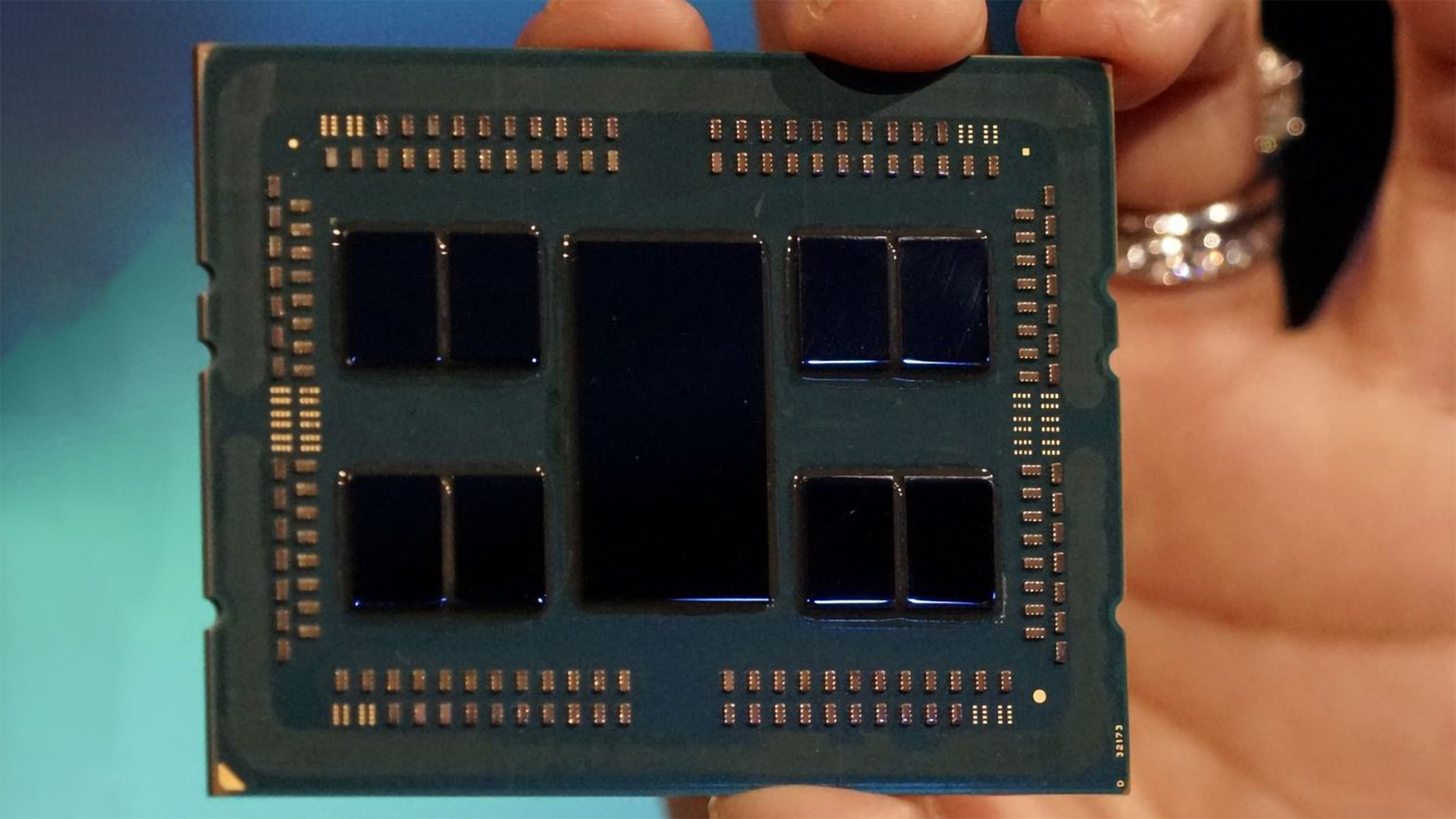
On the CPU side, with Zen 2 and later Zen 3, AMD put the memory controller and PCIe lanes on a central chiplet called the I/O die, along with a high bandwidth interface used to communicate with other chiplets within the package called the Infinity Fabric. These other chiplets so far have consisted of CPU cores with their associated cache, plus the shared L3 cache for the chiplet.
For the consumer CPUs, AMD released processors with one or two CPU chiplets, each of which could have up to eight CPU cores enabled. AMD didn't just create a single I/O chiplet, however, as it wanted to scale up to as many as eight CPU chiplets. Where the consumer I/O die only had Infinity Fabric links for two CPU chiplets, the EPYC and Threadripper variants could link to as many as eight CPU chiplets, providing up to 64-core CPUs like the Threadripper Pro 5995WX and EPYC 7763.
With graphics solutions, you can make the argument that AMD has been toying with chiplet packaging technologies since the Fiji architecture and the R9 Fury X. That was the first product to use HBM (High Bandwidth Memory), with a silicon interposer that helped link together the main GPU core and the HBM stacks.
We wanted to clarify the definition of a "chiplet approach" for GPUs, just to be sure AMD wasn't talking about HBM again. Naffziger confirmed that there would indeed be separate chiplets (not memory chips), though he didn't nail down exactly how AMD will do the split.
Spitballing Possible RDNA 3 Chiplet Designs

Naffziger didn’t tip his hat on the next-gen RDNA 3 architecture, but our best guess is that AMD's GPU chiplet design will likely end up looking at least somewhat like the current CPU designs, where it will have GPU chiplets that house the compute units (CUs), shader cores, and some Infinity Cache. There would then be at least two I/O chiplet designs, one that could scale to higher chiplet counts with a wider memory interface, and one that might only support up to two GPU chiplets with a narrower interface. AMD would link the chiplets via an updated Infinity Fabric, and it would likely have a modest chunk of cache on the I/O chiplet to help optimize memory accesses.
The great thing about the chiplet approach for CPUs is that it enabled excellent economies of scale. For example, the fundamental CPU compute chiplet for Zen 3 houses eight CPU cores and a unified 32MB L3 cache, and it's still only 84mm square in size — less than half the size of Intel's ~215mm square Alder Lake die that's used in the i9-12900K, and almost exactly half the size of the smaller six P-core Alder Lake-S that's estimated at 163mm square. AMD can then put up to eight such chiplets in its top solutions, and yields are excellent considering the die size. It also allows AMD to use the latest process node where it matters most; for example, with Zen 3, the CPU chiplets use TSMC's 7nm node while the I/O chiplet remained on GlobalFoundries' much cheaper 12nm process.
For GPUs, if AMD pulls out all the display interface functionality, video codecs, memory interface, and other general-purpose hardware and just focuses on compute units, it's not too difficult to imagine AMD creating a building block with a 40 CU chiplet that has 2560 (possibly 5120) shader cores and 32–64MB of L3 cache, plus the Infinity Fabric interface. Basically, take Navi 22 (RX 6700 XT), which is a 335mm square chip, and pull out roughly half of the size and put that into the I/O chiplet. Then shrink down the remaining CUs via TSMC's 5nm N5P node and AMD could have a chiplet that's less than 100mm square. Again, yields would be great, and for the consumer sector AMD might have solutions with as many as four such chiplets.
The I/O chiplet would be an entirely different beast. It would house the external memory interfaces, and as such, it could actually benefit by not being on a leading-edge node, meaning AMD could make it on N7 or N6 instead of N5. The I/O interfaces don’t tend to scale well to smaller nodes and external interfaces typically require higher voltages, which can present design challenges with newer nodes. AMD wouldn't have to deal with that as much on an I/O die built on a slightly older process — and it already has the existing GDDR6 interfaces from the various RDNA 2 designs tested and working on TSMC's 7nm process.
The main sticking point with the I/O chiplet would be scaling to the various target markets. A maximum configuration for servers with eight chiplets might seem reasonable, but AMD has bifurcated its consumer and data center designs into RDNA and CDNA, respectively. We already know some of what will go into CDNA 3 and the upcoming Instinct MI300 APU, which will also be used in the El Capitan supercomputer alongside Zen 4 CPUs. RDNA 3 will be quite different, just like RDNA 2 and CDNA 2. In short, we expect AMD will not use the same chiplets for CDNA 3 as it plans for RDNA 3, so scaling up to eight GPU chiplets may be unnecessary.
Instead, AMD could create two I/O chiplets, one for the budget and midrange sectors and a second that would cover high-end and extreme performance graphics cards. Meanwhile, all of the GPU chiplets would be the same core design. That's still a simplification from the current RDNA 2 lineup, where AMD already has four separate chips (Navi 21, 22, 23, and 24), not to mention all the integrated RDNA 2 solutions like Rembrandt and Van Gogh (the Steam Deck processor).
AMD could put a 128-bit memory interface on the smaller I/O chiplet, with defeatured 64-bit or 96-bit variants for lower-tier products, and the ability to link to two GPU compute chiplets. The larger high-end solution could have a 256-bit memory interface (maybe even up to 384-bit), with cut-down options for lower product tiers, and the ability to link up with four, maybe even more, GPU chiplets.
That might sound more complex rather than less complex, but there would be some great advantages. First, the I/O chiplets could be one node behind the leading edge, which would reduce cost, and AMD is already very familiar with designing N7 and N6 products. The smaller I/O chiplet might end up with a die size of around 150mm square (give or take), still smaller than Navi 23, and then it could link up with one or two GPU chiplets as needed. A larger I/O die might be around 225mm square and could use three or four of the same GPU chiplets.
In either case, the total combined die area wouldn't be much worse than a monolithic design but with far better yields. AMD would focus its 5nm production on just a single design, the GPU chiplet, and use the less expensive N6 or N7 wafers for the I/O chiplets. The only trick then is making it all work together properly, and scaling performance with more GPU chiplets.
Other RDNA 3 Architectural Details
Besides the chiplet architecture, we gleaned a few other details about RDNA 3 from our conversation with Naffziger. We asked whether AMD would include some form of tensor core or matrix core in the architecture, similar to what both Nvidia and Intel are doing with their GPUs. He responded that the split between RDNA and CDNA means stuffing a bunch of specialized matrix cores into consumer graphics products really isn't necessary for the target market, plus the FP16 support that already exists in previous RDNA architectures should prove sufficient for inference-type workloads. We'll see if that proves correct going forward, but AMD seems content to leave the machine learning to its CDNA chips.
Another question we had was in regards to Infinity Cache sizes. RDNA 2 had cache sizes ranging from 128MB on Navi 21 down to as little as 16MB on Navi 24, and the resulting gains in performance, even with the smaller cache sizes, were still impressive. With a standard GPU chiplet, AMD might end up ditching the 16MB cache and use 32MB increments, or perhaps it might use even larger cache sizes — or have cache in both the I/O chiplet and the GPU chiplet. Whatever the approach, Naffziger hinted at design decisions where AMD has learned better ways of optimizing the cache use, including excluding certain things that don't tend to benefit from caching (Naffziger mentioned display interface, multimedia processing, and audio processing as being workloads that perhaps don't need to be stored in the Infinity Cache — some of these might get all the cache they need from the L2 cache).
Parting Shots
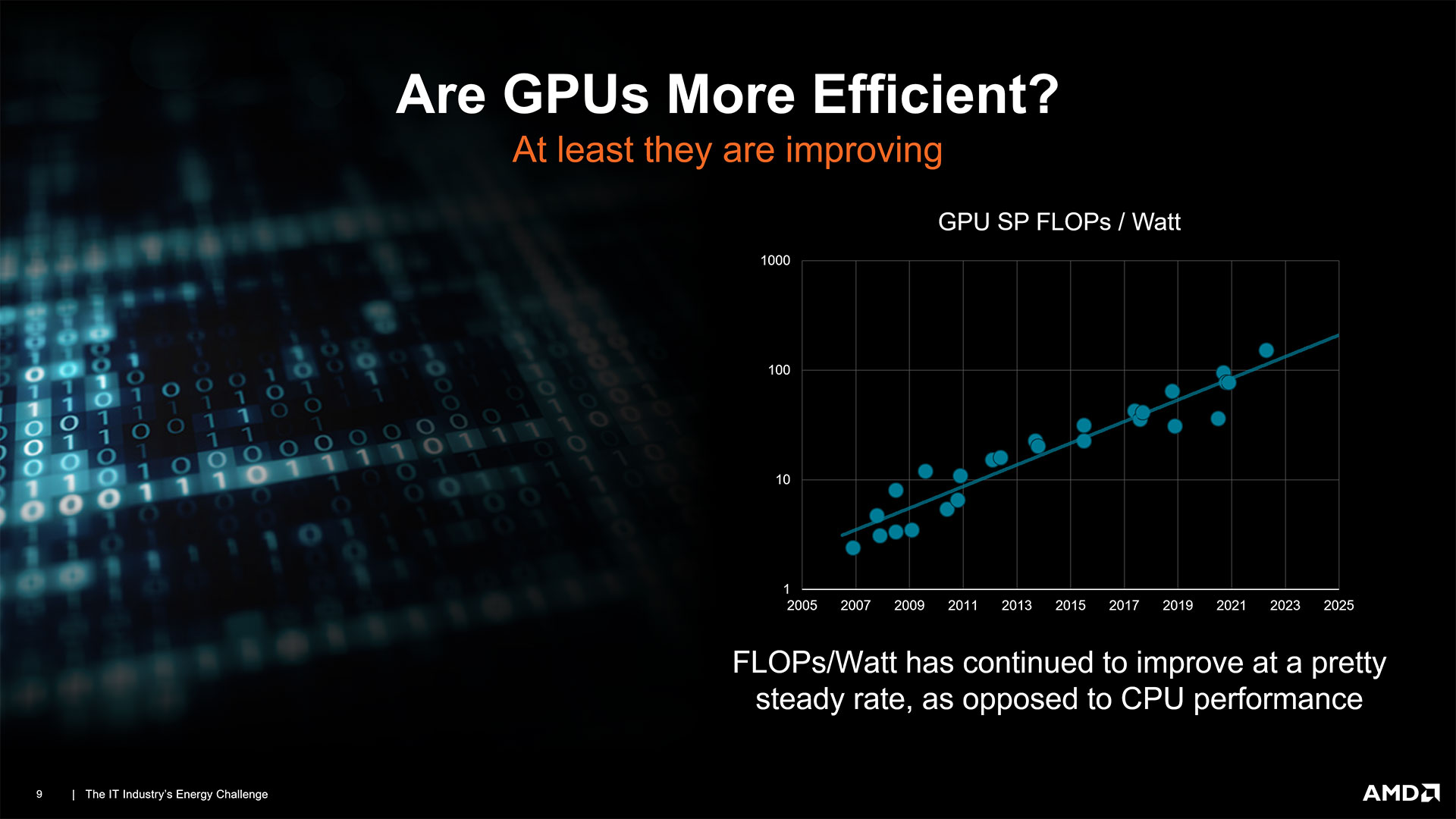
Ultimately, there are a lot of factors that need to be balanced in an architecture like RDNA 3. Moving to chiplets has advantages in economies of scale and allows AMD to move to denser nodes faster than it would be able to otherwise, but there are disadvantages with higher power requirements for the data that gets moved around. Moving data across the Infinity Fabric isn’t free, and, all other factors equal, chiplet-based architectures lose some efficiency during data traversal compared to monolithic designs. As such, care must be taken to ensure a balanced design. AMD has been at the forefront of chiplet designs, with Ryzen CPUs using them for the past three years and EPYC and Threadripper using chiplets since 2017. Each generation has brought improvements in performance and efficiency, and we fully expect AMD to use all of its experience when it shifts to a chiplet-based GPU architecture.
Let's also be clear that while we've made some educated guesses at what AMD might do with RDNA 3, Naffziger was definitely a bit cautious about sharing specific details. We asked at one point whether the chiplets would be similar to Aldebaran (two large dies with a fast interface linking them) or more like the Ryzen CPUs with an I/O chiplet and multiple compute chiplets. The best we could get out of him was a statement that the latter approach was "a reasonable inference" and that AMD would be doing its chiplet-based GPU architecture in "a very graphics-specific way."
Whatever the exact details of the implementation end up being, we're looking forward to seeing RDNA 3 in action later this year. The rumor mill is still swirling with ideas and possibilities, including a potential doubling of the number of FP32 pipelines per compute unit. We also want to see if AMD can still get the desired bandwidth out of a maximum 256-bit memory interface and how the next generation Infinity Cache will turn out.
But more than anything, we want to see another big leap in generational performance. AMD’s approach of focusing on power efficiency, which then allows it to extract more performance at the higher end of the voltage/frequency curve, is a sound design principle. Of course, each type of fundamental design philosophy has its own advantages and disadvantages, and we know that Nvidia also isn’t sitting still — you can expect a fierce battle for both the performance and efficiency crowns when RDNA 3 and the 40-series face off, presumably later this year.
- MORE: Best Graphics Cards
- MORE: GPU Benchmarks and Hierarchy
- MORE: All Graphics Content
Jarred Walton is a senior editor at Tom's Hardware focusing on everything GPU. He has been working as a tech journalist since 2004, writing for AnandTech, Maximum PC, and PC Gamer. From the first S3 Virge '3D decelerators' to today's GPUs, Jarred keeps up with all the latest graphics trends and is the one to ask about game performance.
-
KananX Hopefully AMD will soundly take the performance crown this time, this will help balance the market and prevent Nvidia from demanding atrocious prices for their GPUs again. Also it’s time something changed, just with CPUs back then. Interesting article.Reply -
rluker5 Reply
AMD prices their GPUs on the same price/perf curve as Nvidia. They are both willing participants in the high price duopoly. Your only hope for a disruption in this status quo is Intel GPUs.KananX said:Hopefully AMD will soundly take the performance crown this time, this will help balance the market and prevent Nvidia from demanding atrocious prices for their GPUs again. Also it’s time something changed, just with CPUs back then. Interesting article. -
KananX Reply
No, if AMD is faster, Nvidia can’t do another 3090 stunt with 1500-2000$ msrp. AMD already was cheaper this round, this will not change next round unless AMD is strictly faster and even then, because they are less popular you can expect lower prices than let’s say 3090. If Intel were my hope, I would be hopeless, their GPUs are a trainwreck.rluker5 said:AMD prices their GPUs on the same price/perf curve as Nvidia. They are both willing participants in the high price duopoly. Your only hope for a disruption in this status quo is Intel GPUs. -
Makaveli Replyrluker5 said:AMD prices their GPUs on the same price/perf curve as Nvidia. They are both willing participants in the high price duopoly. Your only hope for a disruption in this status quo is Intel GPUs.
-
waltc3 Nice write up concerning RDNA3, which is naturally limited by what AMD wants to say about it right now, of course....;) Back in 2020, when I first heard Wang discuss splitting off RDNA from CDNA architectures, I was pretty excited. It makes great sense to me. What I got from what he said was that for the gaming segment (RDNA) AMD was removing circuitry not especially tailored for gaming so that they'd have more room in each GPU to support more of the purely gaming circuitry and wouldn't have to devote space to circuitry that isn't as efficient or as robust for gaming as additional RDNA circuitry would be. Since CDNA is more targeted to compute-type processing, as opposed to game & texture acceleration, they could load up the CDNA architecture with more compute-type processing after having removed some of the non-essential gaming circuitry--whatever that may be. I thought it was brilliant and still do. There's definitely a split dynamic for the two types of GPUs presently. That's what I recall from Wang at that time, and it sounds like that's still the plan from your mention of the diverging circuitry in the article. Enjoyed it!...;) Hard to think that we are not quite even half-way through 2022!...;)Reply -
KananX Reply
Essentially AMD copied what Nvidia did with Maxwell back then. Meanwhile Nvidia themselves somewhat deviated from this by using typical things more meant for servers or workstation for gaming cards as well.waltc3 said:Nice write up concerning RDNA3, which is naturally limited by what AMD wants to say about it right now, of course....;) Back in 2020, when I first heard Wang discuss splitting off RDNA from CDNA architectures, I was pretty excited. It makes great sense to me. What I got from what he said was that for the gaming segment (RDNA) AMD was removing circuitry not especially tailored for gaming so that they'd have more room in each GPU to support more of the purely gaming circuitry and wouldn't have to devote space to circuitry that isn't as efficient or as robust for gaming as additional RDNA circuitry would be. Since CDNA is more targeted to compute-type processing, as opposed to game & texture acceleration, they could load up the CDNA architecture with more compute-type processing after having removed some of the non-essential gaming circuitry--whatever that may be. I thought it was brilliant and still do. There's definitely a split dynamic for the two types of GPUs presently. That's what I recall from Wang at that time, and it sounds like that's still the plan from your mention of the diverging circuitry in the article. Enjoyed it!...;) Hard to think that we are not quite even half-way through 2022!...;) -
spongiemaster Reply
Exactly. AMD is no white knight. They want to make just as much money as Nvidia does. The problem is their fanbase won't pay Nvidia prices. Just look at the market now. AMD is offering a game bundle with all their cards and they are still mostly selling below MSRP. Not on the Nvidia side of things. AMD won't release their GPU's before Nvidia releases anything because, AMD wants to let Nvidia set the market. The more Nvidia charges, the more AMD can charge. There is no incentive for them to beat Nvidia to market as it will likely cost them money.rluker5 said:AMD prices their GPUs on the same price/perf curve as Nvidia. They are both willing participants in the high price duopoly. Your only hope for a disruption in this status quo is Intel GPUs. -
escksu ReplyKananX said:No, if AMD is faster, Nvidia can’t do another 3090 stunt with 1500-2000$ msrp. AMD already was cheaper this round, this will not change next round unless AMD is strictly faster and even then, because they are less popular you can expect lower prices than let’s say 3090. If Intel were my hope, I would be hopeless, their GPUs are a trainwreck.
Not going to work. This is because AMD is holding just around 17% of the market. It's around 1/5 that of Nvidia. Of course we have hpc sector but that's a different thing.
Btw, you won't see any price war in GPU nor CPU sector. Because there are literally just 2 companies (waiting for Intel to become 3rd) in the market, they will never enter a pricing competition.
What they all will do instead is to offer similar products at similar prices. -
KananX Reply
Then you didn’t really follow what happened the last decades. Every time AMD was faster it pushed down Nvidias prices by a lot and also forced them to release faster GPUs for a lower price. Exactly what also happened with the 3080 last gen.escksu said:Not going to work. This is because AMD is holding just around 17% of the market. It's around 1/5 that of Nvidia. Of course we have hpc sector but that's a different thing.

