AMD Ryzen 5 3500X Rivals Intel Core i5-9400F in Early Listing
Chinese retailer JD.com has listed the AMD Ryzen 5 3500X on its online store. The processor is in all likelihood the older brother of the previously leaked AMD Ryzen 5 3500.
AMD is looking pretty serious about trying to steal some of Intel's market share in the budget CPU market. The latest listing shows that the Red Team isn't just working on the Ryzen 5 3500 as a budget chip, but the Ryzen 5 3500X as well.
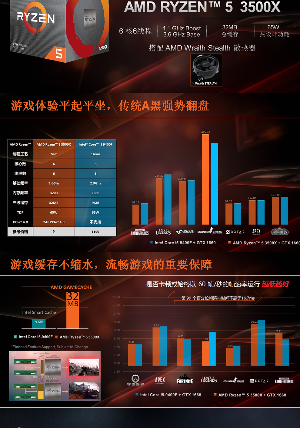
JD.com lists the Ryzen 5 3500X as a six-core, six-thread processor with a 3.6 GHz base clock, 4.1 GHz boost clock, 65W TDP (thermal design power) and 32MB of L3 cache. If you've been following AMD's Matisse rumors, the Ryzen 5 3500X's specifications are almost identical to those of the Ryzen 5 3500, except the latter is rumored to only have 16MB of cache. AMD will seemingly the Wraith Stealth CPU cooler with the Ryzen 5 3500X.
Specs
| Model | Cores / Threads | Base Clock | Boost Clock | L3 Cache | TDP | PCIe Lanes | Memory Support | MSRP |
| AMD Ryzen 5 3500X* | 6 / 6 | 3.6 GHz | 4.1 GHz | 32MB | 65W | PCIe 4.0 x 24 | Dual DDR4-3200 | ? |
| AMD Ryzen 5 3500* | 6 / 6 | 3.6 GHz | 4.1 GHz | 16MB | 65W | PCIe 4.0 x 24 | Dual DDR4-3200 | ? |
| Intel Core i5-9400F | 6 / 6 | 2.9 GHz | 4.1 GHz | 9MB | 65W | PCIe 3.0 x 16 | Dual DDR4-2666 | $182 |
*Specifications in the table are unconfirmed
Based on the marketing material from JD.com, the Ryzen 5 3500X specifically targets the Intel Core i5-9400F. Both processors share the same core count, boost clocks and TDP rating, but that's where the similarities end. On paper, the Ryzen 5 3500X has the upper-hand, with a 700 MHz higher base clock, 23MB more L3 cache, not to mention native support for the PCIe 4.0 interface and DDR4-3200 memory modules.
The JD.com listing also includes real-world gaming results between the Ryzen 5 3500X and Core i5-9400F. The processors were said to be paired with the Nvidia GeForce GTX 1660 graphics card for the tests. The charts say that the Ryzen 5 3500X's gaming performance is in the same ballpark as the Core i5-9400F. What we'd like really love to see, though, is how the Ryzen 5 3500X fares against the Core i5-9400F in a office, rendering or productivity environment as that's where AMD's chip could really shine.
The Ryzen 5 3500X's success will depend hugely on how AMD prices the six-core chip. Intel's Recommended Customer Price (RCP) for the Core i5-9400F is $182. However, we can usually find it on sale for $139.99. The price for the Ryzen 5 3500X on JD.com is 1,099 yuan, which converts to $155. There's also the more powerful AMD Ryzen 5 3600 selling for $199. If AMD could match the price of the Core i5-9400F, it'll be strong competition for the Intel chip.
Get Tom's Hardware's best news and in-depth reviews, straight to your inbox.

Zhiye Liu is a news editor, memory reviewer, and SSD tester at Tom’s Hardware. Although he loves everything that’s hardware, he has a soft spot for CPUs, GPUs, and RAM.
-
jimmysmitty I really wish they would write the specs better. Stating 24 PCIe lanes is a bit misleading. It has 24 total but 4 are used for the link to the chipset so that leaves 20 lanes. Of that 16 are dedicated to graphics with the other 4 typically set to be used for NVMe, by most motherboard manufactures. If they want to do it that way then they should also list the i5 as having 20 since it has 16 for graphics and 4 for DMI, the link to the chipset.Reply
I also love the marketing terms like "Gamecache". 32MB seems a bit much and would take up a lot of die space. I doubt it will provide any tangible gaming performance gains but guess we will have to wait and see.
Ahhh marketing. It never fails to amuse. -
InvalidError Reply
The 32MB "gamecache" is the same as the 3600-3800 and AMD needs it, along with the doubling of L2 caches, to mitigate the impact of chiplets having 10-20ns worse memory latency than 2nd-gen Ryzen.jimmysmitty said:I also love the marketing terms like "Gamecache". 32MB seems a bit much and would take up a lot of die space. I doubt it will provide any tangible gaming performance gains but guess we will have to wait and see. -
jimmysmitty ReplyInvalidError said:The 32MB "gamecache" is the same as the 3600-3800 and AMD needs it, along with the doubling of L2 caches, to mitigate the impact of chiplets having 10-20ns worse memory latency than 2nd-gen Ryzen.
That latency is due to the IMC being on a chiplet instead of the CPU die, correct? So the cache is more of a way to make sure it performs at least on par in that regard.
Still marketing is great. What a name for it. -
InvalidError Reply
Pretty much.jimmysmitty said:That latency is due to the IMC being on a chiplet instead of the CPU die, correct? So the cache is more of a way to make sure it performs at least on par in that regard.
I don't think the IMC moniker still applies to Zen 2 though as memory controllers got divorced from CPU cores and now reside in the on-package north bridge / MCH. -
jimmysmitty ReplyInvalidError said:Pretty much.
I don't think the IMC moniker still applies to Zen 2 though as memory controllers got divorced from CPU cores and now reside in the on-package north bridge / MCH.
I would agree. Sort of odd they would move the MC to the chiplet. I would think they would want the MC on the CPU die and the rest on the chiplet as memory latency is always a key issue. However it might have helped the cores themselves in terms of power draw and overall temperatures so there was probably a benefit.
I am not sure Intel will ever do that. I can see them pulling I/O off onto a on package chip but the MC is always the one that gets effected most by latency. -
InvalidError Reply
Not really that odd. Memory is just one particular type of IO and just like any other IO, the front-end circuitry does not scale much with process. Also, one major problem with giving each CPU chiplet its own local memory is heavier performance penalties when cores need to access non-local memory, which is particularly troublesome for consumer software generally oblivious to memory layout. Centralizing all memory controllers in the IO die eliminates issues with non-uniform memory access, albeit at the expanse of 10-20ns worse memory latency for every core.jimmysmitty said:Sort of odd they would move the MC to the chiplet.
Since optimizing for one subset of workloads often requires beefing parts of the architecture that may be detrimental to other workloads, such as accommodating workloads with larger cache footprint with larger caches at the expense of increased L2/L3 latency which is detrimental to workloads with small cache footprint that benefit more from low latency, it is impossible to design a chip that is simultaneously superior in every measurable way.
CPU design has always been a game of compromises. -
jimmysmitty ReplyInvalidError said:Not really that odd. Memory is just one particular type of IO and just like any other IO, the front-end circuitry does not scale much with process. Also, one major problem with giving each CPU chiplet its own local memory is heavier performance penalties when cores need to access non-local memory, which is particularly troublesome for consumer software generally oblivious to memory layout. Centralizing all memory controllers in the IO die eliminates issues with non-uniform memory access, albeit at the expanse of 10-20ns worse memory latency for every core.
Since optimizing for one subset of workloads often requires beefing parts of the architecture that may be detrimental to other workloads, such as accommodating workloads with larger cache footprint with larger caches at the expense of increased L2/L3 latency which is detrimental to workloads with small cache footprint that benefit more from low latency, it is impossible to design a chip that is simultaneously superior in every measurable way.
CPU design has always been a game of compromises.
What would you say to stacked or on die memory? -
InvalidError Reply
On-die DRAM is generally a no-go since the low leakage current process tech required to make DRAM is not compatible with high-speed logic. You can make logic on DRAM process if you don't mind much lower clock frequencies.jimmysmitty said:What would you say to stacked or on die memory?
If you stack memory on CPU chiplets to use as local RAM and have more than one such stack in a CPU, you will run into the same NUMA issues as before, albeit with lower overall latencies due to the direct connection between the chiplet's IMC and stacked DRAM, if the OS isn't making sure to keep most data dependencies for processes running on a given core in the appropriate chiplet's RAM address space. -
MasterMadBones ReplyInvalidError said:If you stack memory on CPU chiplets to use as local RAM and have more than one such stack in a CPU, you will run into the same NUMA issues as before, albeit with lower overall latencies due to the direct connection between the chiplet's IMC and stacked DRAM, if the OS isn't making sure to keep most data dependencies for processes running on a given core in the appropriate chiplet's RAM address space.
That's true, but to me it doesn't sound entirely unrealistic for AMD to make an on-package L4 cache somewhere in the future. That would be tied directly to the IO die, not to any of the CCDs. We've seen L4 caches before and they were not so effective, but as a method to bridge the large gap between the different L3 slices and DRAM, a single 2-8Gb DRAM die could prove very useful. -
InvalidError Reply
The main problem with DRAM as L4 cache is that DRAM of any type of external interface still has a ~10ns latency of its own from CAS to first data read, still has hefty penalties from having to rewrite the row data register back into DRAM cells whenever you want to address a different memory row since reading DRAM cells is destructive, still requires periodic refresh of every row, etc. A third issue is that having another tier of tag-RAM and cache for memory requests to filter through will increase total latency for everything that ultimately winds up in the memory controller queues.MasterMadBones said:That's true, but to me it doesn't sound entirely unrealistic for AMD to make an on-package L4 cache somewhere in the future.
Intel's 64-128MB eDRAM on Haswell-Skylake chips with Iris Pro IGP did wonders for IGP performance and workloads with core datasets larger than L3 yet smaller than L4. Hurt most other things so Intel scrapped it along the move to DDR4.
The more likely outcome for embedded memory is that we'll have CPUs with 16+GB of embedded memory to run the system on and optional external DRAM/NVDIMM as a very-high-speed (50+GB/s) swapfile.

