Intel: Xe-HP GPU Now Available to Developers, Xe-HPC GPU Development Finished
Intel's Xe graphics odyssey continues as Xe-HP & Xe-HPC hit new milestones.

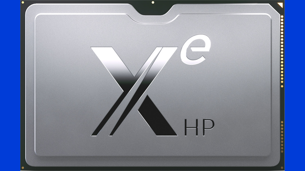
Intel this week provided some updates regarding the progress of its ultra-high-end Xe graphics processors. As it turns out, the company's Xe-HP GPU for datacenters is now available to select developers, whereas the development of Intel's Xe-HPC for supercomputers has been finished and the chip giant is awaiting the device back from the fab after it released the first revision to manufacturing.
The Xe-HP: It's All About Scalability
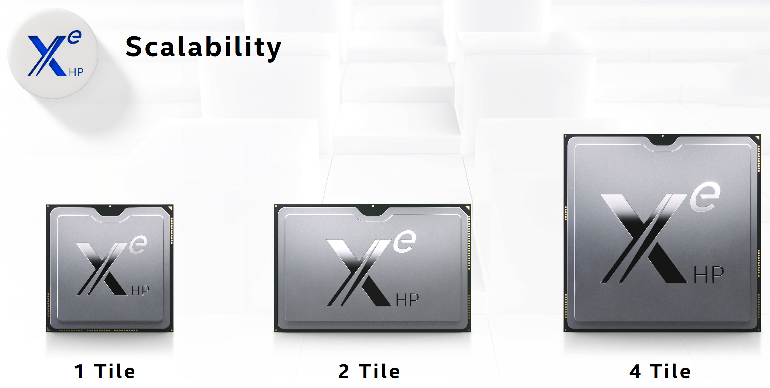
Intel's Xe-HP is all about massive scalability of everything that the company's Xe-LP architecture (used for the 11thGeneration Core CPUs (Tiger Lake) CPU and the Iris Xe Max discrete GPU) has to offer. This includes overall performance, compute capabilities, media encoding/decoding capabilities, memory bandwidth, and power consumption.
The Xe-HP architecture uses different execution units (EUs) than the Xe-LP architecture. These EUs support data formats and instructions common for data centers and high-performance computing (HPC), which includes FP64 for technical computing, bfloat16 for AI/ML workloads, DP4A convolution instruction for DL, and Intel’s new XMX instructions.
Intel once confirmed that Xe-HP GPUs would have 'quad-digit numbers' of EUs, these EUs have IPC improvements over the current-generation Xe-LP designs, and they also run at 1.5 ~ 2X the frequency of Xe-LP (i.e., at least 2.0 ~ 2.5 GHz if we take Tiger Lake's iGPU as a reference point). Intel used an all-new fabric for internal interconnections to support a massive increase in the number of execution units. Also, the Xe-HP uses HBM-type memory connected with Intel's EMIB technology.
The Xe-HP GPUs for data centers will be made using Intel's 10nm Enhanced SuperFin process technology. The graphics processors will support a multi-tile architecture, and the company plans to offer at least three versions of its datacenter GPU: with one tile, two tiles, and four tiles. The top-of-the-range model might end up consuming up to 500 Watts.
Intel taped out one of the first Xe-HP around mid-2020 and then demonstrated early silicon running at undisclosed (presumably low) clocks in August. That early Xe-HP GPU provided performance of around 40 FP32 TFLOPS, which is two times more FP32 throughput than Nvidia’s A100 graphics processor.
After testing its Xe-HP silicon internally for months, the company recently started to make this part available to select developers in a bid to enable them to prepare their software for a large-scale Xe-HP deployment. It is unclear whether Intel has actually shipped its Xe-HP GPUs to developers physically, or just has started to let them access the hardware remotely. Anyhow, Intel’s Xe-HP GPU is now good enough for developers, which is a positive sign.
Get Tom's Hardware's best news and in-depth reviews, straight to your inbox.
The Xe-HPC: A Supercomputing Powerhouse
Intel’s Xe-HPC is the company’s most advanced version of its Xe architecture known to date with enhancements specific to supercomputers (so expect instructions beyond what the Xe-HP offers).
The only Xe-HPC GPU announced by Intel so far is the codenamed Ponte Vecchio compute processor that will, among other things, power the upcoming exascale Aurora supercomputer. In addition to features and performance, the Ponte Vecchio GPU will be extremely complex and consist of four heterogeneous tiles packed and interconnected using Intel’s Foveros and Co-EMIB technologies.
At its recent press briefing, Intel confirmed that it has 'released the first revisions of all chiplet designs to manufacturing and are eagerly awaiting their arrival to power on,' for the first Xe-HPC GPU, meaning that its development is finished. Meanwhile, the company did not explicitly said it was the Ponte Vecchio. Right now, Intel is expecting the chip from the fab.
Since Intel's 7 nm process technology got delayed by about six months, Intel said this summer that it would produce Ponte Vecchio's compute tile both internally and externally. Intel did not disclose where the first Xe-HPC compute tile silicon would be made and using which fabrication technology. Meanwhile, porting a design developed for a particular manufacturing process to another one usually leads to rather unpredictable results when it comes to power.
Due to a lack of information from Intel, it isn't wise to speculate where the company plans to tape out the compute tile of the Ponte Vecchio (or the fi), but this will certainly be an interesting thing to learn eventually.
Summary
From a development standpoint and based on Intel's information, Intel's Xe-HP and Xe-HPC projects are proceeding fine. The Xe-HP GPU works well enough to offer it to developers, whereas the Xe-HPC development has been finished about 1.5 years before its projected launch date.
Intel yet has to tape out the first Xe-HPC silicon and pass all the verifications specific to the bring-up process. Furthermore, only time will tell whether Intel can introduce commercial versions of its Xe-HP and Xe-HPC products on time, and if they will meet performance and power goals set by the company.

Anton Shilov is a contributing writer at Tom’s Hardware. Over the past couple of decades, he has covered everything from CPUs and GPUs to supercomputers and from modern process technologies and latest fab tools to high-tech industry trends.
-
JayNor Xe-HPG has already been back in the lab for a few months. Leaks indicate it was built in N6 EUV at tsmc.Reply
Intel has also been building Mobileye eyeq5 parts in tsmc 7nm since 2018, has been sampling since then and plans to ramp to volume production in 2021. -
JayNor I don't believe Intel announced any delays in their 7nm processing for GPUs ... only for the CPUs that were previously scheduled for 2022.Reply


