Nvidia RTX 4080/4090's Power-Hungry PCB Design Allegedly Detailed
Enthusiast-grade Ada Lovelace graphics cards are expected to be huge.

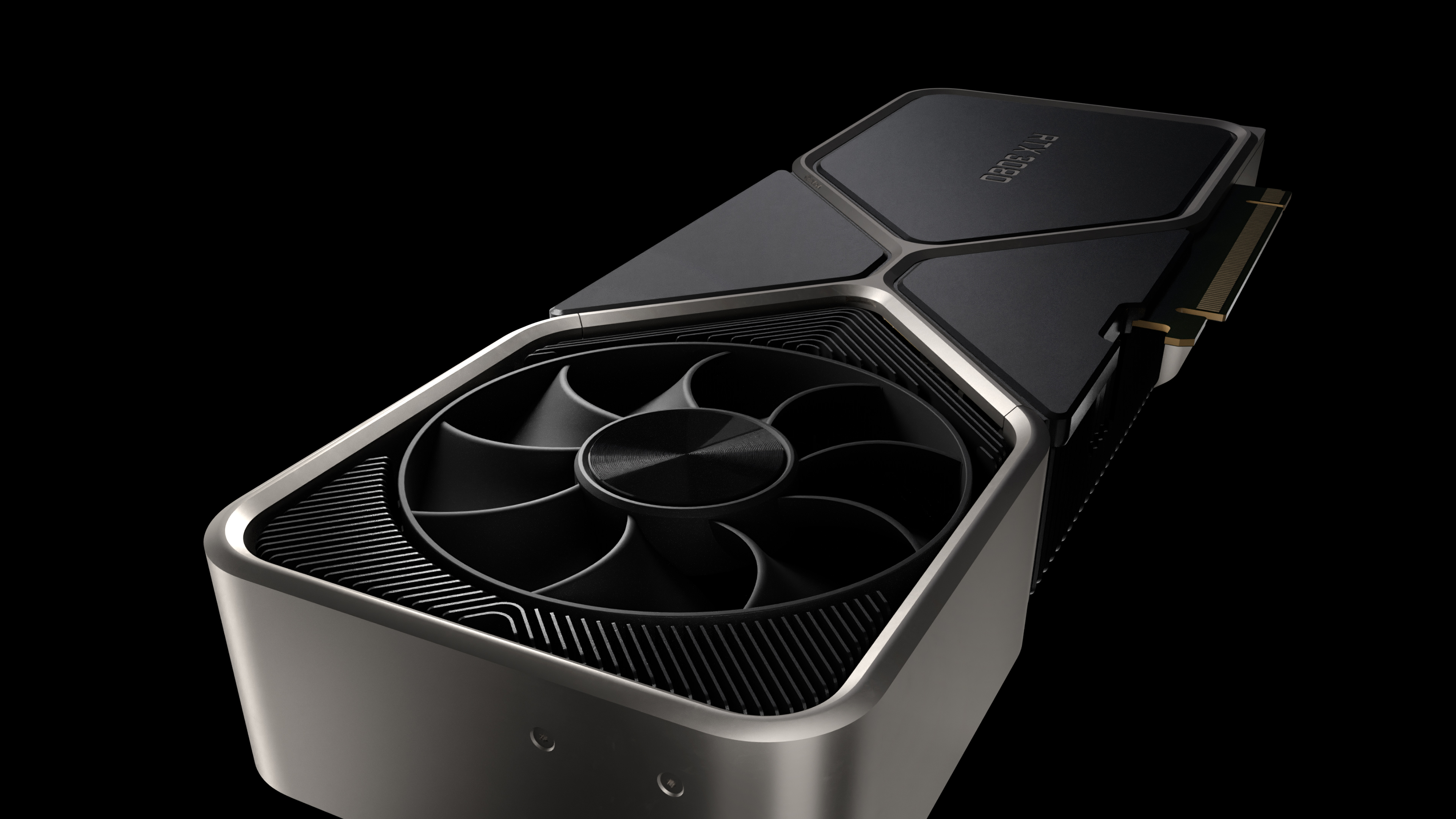
An early look at the printed circuit board (PCB) design for Nvidia's next-generation GeForce RTX 4080 and RTX 4090 reveals that the forthcoming graphics boards will continue to be huge and power-hungry. A new report claims that makers of graphics cards will be able to re-use PCBs developed for the GeForce RTX 3090 Ti for their next-generation products.
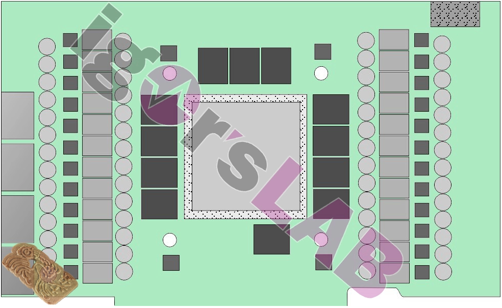
Reference design of graphics cards based on Nvidia's codenamed AD102 graphics processing units can accommodate up to 12 GDDR memory chips, so the GPU will support memory interfaces of up to 384-bits, according to Igor's Lab. The information was indirectly confirmed by @kopite7kimi, who tends to have some accurate details about upcoming products. With up to 12 memory chips, Nvidia's GeForce RTX 4080/4090 graphics cards will be able to house up to 24GB of memory using 16Gb (2GB) DRAM ICs, so expect memory configurations of next-generation boards to be like those available now.
Nvidia's GeForce RTX 4080/4090 reference design for add-in-board manufacturers reportedly has a complicated multi-phase voltage regulating module that uses uPI Semi's UP9512 multiple phase buck controllers. Igor's Lab, which schematically reproduced the said PCB design, claims that the card will use a 12VHPWR (12+4-pin) auxiliary PCIe 5 power connector and consume up to 600W. For those who do not have a modern ATX 3.0-compliant PSU, Nvidia and its partners are expected to bundle 4x8-pin to 12VHPWR adapters with the boards.
While graphics cards are getting larger and more power-hungry, 600W of heat in a client system is not easy to reliably take away even using liquid cooling. Meanwhile, Nvidia's Founders Edition and reference design boards are expected to retain a triple-slot air cooler. However, some custom-designed products are projected to employ a 3.5-wide cooling system, possibly to improve reliability and/or provide some additional overclocking headroom.
Nvidia is expected to use TSMC's 4N fabrication process (a custom Nvidia-specific node) to build its next-generation Ada Lovelace GPUs. So, it is somewhat illogical for these parts to be considerably more power-hungry than Ampere GPUs produced using Samsung's outdated N8 manufacturing technology, even keeping in mind an increase in transistor count. Still, we are somewhat skeptical about a 600W thermal board power (TDP) for next-gen graphics products.
Igor's Lab further indicates that Nvidia's GA102 and AD102 GPUs are pin-to-pin compatible, so makers of graphics cards can re-use their GeForce RTX 3090 Ti PCB designs (probably with some upgrades) for their next-generation products. If the report is accurate, it may be the first time in history that high-end GPUs of completely different generations using different fabrication processes are pin-to-pin compatible and can use the same PCB designs.
With entry-level, mainstream, and notebook parts, companies tend to maintain pin-to-pin compatibility since notebook makers are not very eager to redesign their motherboards every year. However, with higher-end desktop GPUs, developers tend to rework PCB design with each generation to adjust it to s new GPU design, maximize performance, and optimize cooling.
Get Tom's Hardware's best news and in-depth reviews, straight to your inbox.
For now, any information about Nvidia's GeForce RTX 4080/4090 graphics cards based on Ada Lovelace GPUs should be taken with a grain of salt as they are still months away from introduction. Nonetheless, some details that leak today may well be correct.

Anton Shilov is a contributing writer at Tom’s Hardware. Over the past couple of decades, he has covered everything from CPUs and GPUs to supercomputers and from modern process technologies and latest fab tools to high-tech industry trends.
-
hotaru251 I do wonder how they will deal with future where they are too hot to cool with modern cooling.Reply
Do they just stop making new gpu's at that point?
Do they have to have massive quad slot cooling? -
sizzling Replyhotaru251 said:I do wonder how they will deal with future where they are too hot to cool with modern cooling.
Do they just stop making new gpu's at that point?
Do they have to have massive quad slot cooling?
I seem to recall wasn’t there a problem in one US state with OEM systems using over a certain amount of power? I know several years back the EU were looking into possibly putting power limits on domestic PC’s. In a world where energy usage and associated emissions is becoming more heavily scrutinised I do wonder if requirements go up for next gen cards if the home PC industry will see new regulations imposed in some countries across the globe. -
peachpuff Reply
Lower clock and more cores?hotaru251 said:I do wonder how they will deal with future where they are too hot to cool with modern cooling.
Do they just stop making new gpu's at that point?
Do they have to have massive quad slot cooling? -
hotaru.hino Reply
The limits were on how much power they consume at idle. However, I'm not too convinced this may be a problem still even if the card consumes 500W. For instance, I can get my RTX 2070 Super to idle at 20W and thought maybe my GT 1030 would be significantly better. Sure, from a percentage point of view it is at ~13W, but from an absolute perspective it's a pittance.sizzling said:I seem to recall wasn’t there a problem in one US state with OEM systems using over a certain amount of power? I know several years back the EU were looking into possibly putting power limits on domestic PC’s. In a world where energy usage and associated emissions is becoming more heavily scrutinised I do wonder if requirements go up for next gen cards if the home PC industry will see new regulations imposed in some countries across the globe.
On a tangent, the only reason why I think this is a thing is because people leave their computers on all the time even if they're not using them. In some of the articles they mentioned a typical gaming PC consumes 63KWHr a year idling. -
hotaru251 Reply
CA and only for prebuilts stock settigns & idle. nothing to do with person OC'ing it after.sizzling said:I seem to recall wasn’t there a problem in one US state with OEM systems using over a certain amount of power?
still hit point where it wont be an improvement in performance and still require more cooling than will fit in most rigs.peachpuff said:Lower clock and more cores? -
sizzling Reply
but it goes to show power consumption of home PC’s is already being scrutinised by governments.hotaru251 said:CA and only for prebuilts stock settigns & idle. nothing to do with person OC'ing it after.
. -
King_V Ok, this is weird... is Nvidia getting lazy? Are they going to have THAT much more performance that more than justifies the increased power consumption, or are they just cranking up the wick and damn the torpedoes?Reply -
peachpuff Reply
But it's the inefficiencies of higher clocks that cause excessive power drain, that's why amd has low clocked 64core cpus that only use 280w while higher clocked consumer 8core cpus use a third of that. Sure single cpu workloads suffer but gpu don't have that issue.hotaru251 said:
still hit point where it wont be an improvement in performance and still require more cooling than will fit in most rigs. -
jacob249358 Reply
yeah but that's just California. They are VERY liberal and its probably about climate change or something.sizzling said:but it goes to show power consumption of home PC’s is already being scrutinised by governments. -
hotaru.hino Reply
To be fair, desktop parts simply ship with "performance at all costs" mindset. With a bit of undervolting and tweaking, you can get these parts to consume like 80% of their marketed TDP with minimal performance loss.King_V said:Ok, this is weird... is Nvidia getting lazy? Are they going to have THAT much more performance that more than justifies the increased power consumption, or are they just cranking up the wick and damn the torpedoes?
