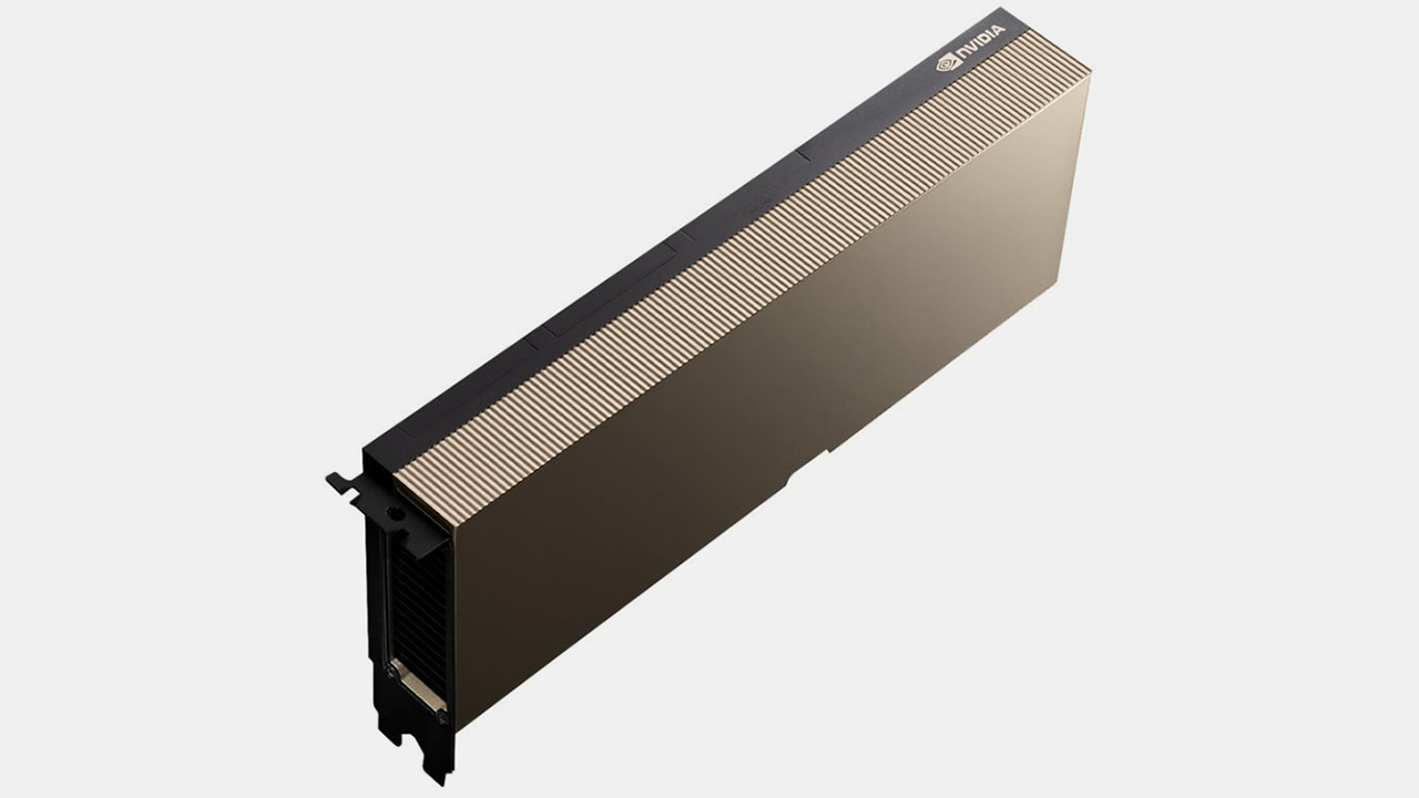
Nvidia's H100 Hopper Compute GPU Benchmarked in Games, Found Lacking
Nvidia's H100 can do computing, but cannot do gaming.

Although compute GPUs like Nvidia's H100 formally belong to the category of graphics processing units, they can barely render graphics as they do not have enough special-purpose hardware. As it turns out Nvidia's H100, a card that costs over $30,000 performs worse than integrated GPUs in such benchmarks as 3DMark and Red Dead Redemption 2, as discovered by Geekerwan.
Nvidia's H100 card is based on the company's GH100 processor with 14,592 CUDA cores that support a variety of data formats used for AI and HPC workloads, including FP64, TF32, FP32, FP16, INT8, and FP8. By contrast, Nvidia's consumer GPUs, such as Nvidia's AD102, only properly support FP32. Meanwhile, GH100 only has 24 raster operating (ROPs) units and does not have display engines or display outputs. Furthermore, Nvidia does not optimize Hopper drivers for gaming applications.
But apparently it is still possible to make Nvidia's H100 render graphics and even support ray tracing. Only it renders graphics rather slowly. One H100 board scores 2681 points in 3DMark Time Spy, which is even slower than performance of AMD's integrated Radeon 680M, which scores 2710.
But running games on a card that costs over $30,000 does not make a lot of sense and Nvidia certainly did not design GH100 for rendering graphics. While Nvidia's GH100 has some graphics specific hardware inside, it is not made to offer any substantial performance in games, which is why it is slower than AMD's integrated Radeon 680M.
Although Nvidia's flagship compute GPU is not meant for graphics, it outperforms everything in datacenter AI and HPC applications and this is exactly what it is made for.
Get Tom's Hardware's best news and in-depth reviews, straight to your inbox.

Anton Shilov is a contributing writer at Tom’s Hardware. Over the past couple of decades, he has covered everything from CPUs and GPUs to supercomputers and from modern process technologies and latest fab tools to high-tech industry trends.
-
H100 is actually structured so that only 2 of its TPCs/(Texture Processing Clusters are available for the standard graphics processing tasks, while the entire GPU block is primarily dedicated to compute tasks so that can lead to adverse results in gaming.Reply
The poor performance was due to under-utilization and the non-optimized nature of the drivers which should be expected since the H100 is an HPC/AI-first solution and the company has no official gaming drivers made for the card.
We can also see that the power of the card is under 100W, which means it is having major under-utilization of the H100 GPU in games. -
It appears that the tester was actually running the chip on a standard PC in a 4-Way configuration.Reply
For testing a 3D-Printed duct had to be made to deliver cooling to the card, since it comes with a passive heatsink which means there's no active cooling solution onboard the card.
It was not necessary to use a 4-way setup at least to test games, IMO. For display he had to use the GTX 1650 Ti graphics card as a secondary display card, since the H100 lacks display outputs.
If you watch the video carefully, it looks like using two H100s offered a 43% boost in content creation apps, but, 3-way and 4-way results showed diminishing returns and negative scaling. Looks like standard PCs just can't take advantage of multiple H100 GPUs.
-
bit_user Reply
Similar to the A100, from what I'd heard. My guess is that Nvidia wanted to enable some degree of OpenGL support for HPC users to visualize the data from their simulations.Metal Messiah. said:H100 is actually structured so that only 2 of its TPCs/(Texture Processing Clusters are available for the standard graphics processing tasks, while the entire GPU block is primarily dedicated to compute tasks so that can lead to adverse results in gaming.
AMD has gone to the extreme, with their CDNA architecture, and completely omitted texturing, ROPs, etc.
In that picture, there's no over-the-top connectivity (i.e. NVLink) being used. Was there, in the video?Metal Messiah. said:If you watch the video carefully, it looks like using two H100s offered a 43% boost in content creation apps, but, 3-way and 4-way results showed diminishing returns and negative scaling. Looks like standard PCs just can't take advantage of multiple H100 GPUs.
Also... OMG, Legos!
(lower left) -
Replybit_user said:Similar to the A100, from what I'd heard. My guess is that Nvidia wanted to enable some degree of OpenGL support for HPC users to visualize the data from their simulations.
AMD has gone to the extreme, with their CDNA architecture, and completely omitted texturing, ROPs, etc.
In that picture, there's no over-the-top connectivity (i.e. NVLink) being used. Was there, in the video?
Also... OMG, Legos!
(lower left)
Yes, NVidia only enabled two TPCs in both the SXM5 and PCIe H100 GPUs which are graphics-capable, so that they can run vertex, geometry, and pixel shaders, which means 2 TPCs (4 SMs) out of 57 TPCs (114 SMs).
But by tradition, Nvidia still calls the H100 a graphics processing unit, but the term is clearly on its last legs: because just two out of the 50+ texture processing clusters (TPCs) in the device are actually cable of running vertex, geometry, and pixel shader maths required to render 3D graphics.
Hey, is that a real LEGO ? :smiley: