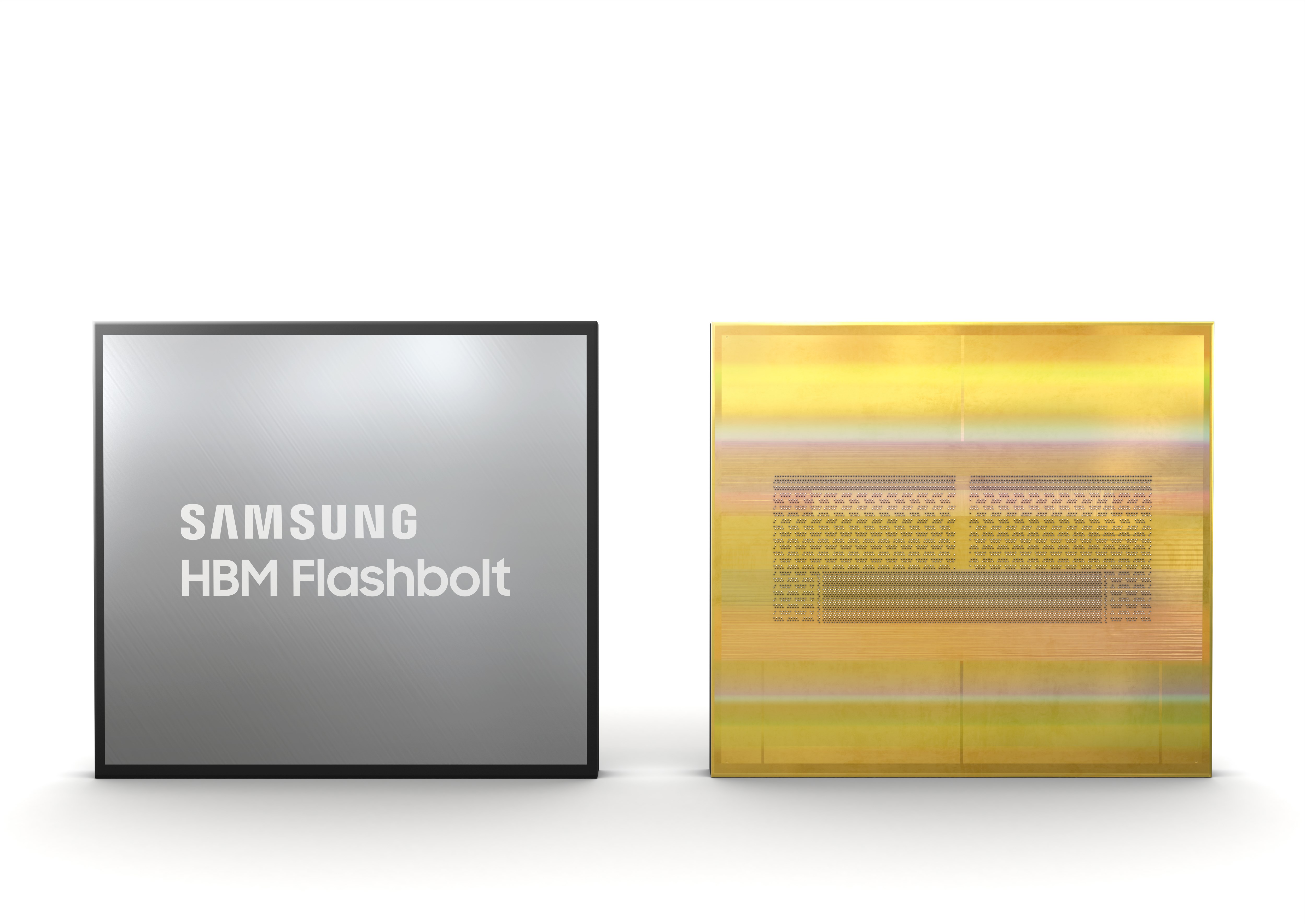
Samsung Preps Mass Production of Flashbolt HBM2E DRAM
Flashbolt packs 16GB of DRAM onto one tiny package targeting high-performance computing.

When high bandwidth memory (HBM) launched in 2015, there were high hopes for it, but it was still too immature to compete with the GDDR5 memory popular with graphics cards at the time. This changed quickly with the arrival of HBM2. Now, five years after the introduction of HBM's first generation, Samsung is the first to announce mass production of third-generation HBM2E memory. Flashbolt, which Samsung first revealed at Nvidia's GTC event in March, will see mass production in the first half of 2020.
By stacking DRAM dies, HBM in general allows for the realization of a much wider memory bandwidth (as seen by the Flashbolt's 1,024-bit bus). As a result, a tiny package can achieve a very high bandwidth. This is useful for integrating onto the GPU chips themselves, saving valuable space on a graphics card's printed circuit board.
Since originally announcing Flashbolt in March, Samsung hasn't changed any of its specifications, which include eight 16 gigabit (Gb) dies stacked on top of one another to create a 16GB memory stack.
At 3,200 MHz, Flashbolt offers a memory transfer speed of 410 GBps with its 1,024-bit memory interface. Nevertheless, Samsung has tested the memory to run at up to 4,200 MHz, which brings the bandwidth all the way up to a massive 538 GBps, telling us that HBM2E might have some great overclocking potential.
Article continues belowIn comparison, the previous-generation HBM2 memory 'Aquabolt' from Samsung offered a total capacity of 8GB, ran at 2,400 MHz and had a maximum bandwidth of 307.2 GBps per stack.
The DRAM used is built on 10nm lithography, and the package uses 40,000 Through-Silicon Via's (TSV). Each of the eight 16Gb dies has 5,600 microbumps.
“With the introduction of the highest performing DRAM available today, we are taking a critical step to enhance our role as the leading innovator in the fast-growing premium memory market,” said Cheol Choi, EVP of Memory Sales & Marketing at Samsung, said in a statement accompanying today's announcement. “Samsung will continue to deliver on its commitment to bring truly differentiated solutions as we reinforce our edge in the global memory marketplace.”
HBM2E memory isn't immediately aimed at consumer products, but it's possible it could end up in a handful of consumer-facing offerings, just like how the AMD Radeon VII (16GB) came with two HBM2 stacks. The primary target of HBM2E, however, is high-performance computing (HPC) and supercomputers.
Get Tom's Hardware's best news and in-depth reviews, straight to your inbox.
Given the timing of this release, it wouldn't come as a surprise to see Nvidia's next-generation HPC Tesla GPUs pack Flashbolt memory. We already know that Indiana University postponed GPU installation in its supercomputer to wait for the 70-75% performance increase from the successor to Volta-based Tesla V100 GPUs. This successor, likely called the Tesla A100, will be based on the Ampere architecture, which Nvidia could announce at its GTC keynote on March 23.
Samsung will continue to offer Aquabolt while Flashbolt awaits mass production.
Niels Broekhuijsen is a Contributing Writer for Tom's Hardware US. He reviews cases, water cooling and pc builds.
-
jimmysmitty It wasn't so much that it wasn't mature it was more the cost was too much compared to GDDR5.Reply
