TSMC Kicks Off 3nm Production: A Long Node to Power Leading Chips

Wafer
(Image credit: Shutterstock)

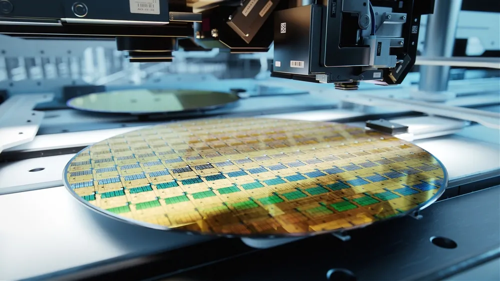
TSMC on Thursday held a "Volume Production and Capacity Expansion Ceremony" at its Fab 18 in in the Southern Taiwan Science Park (STSP). Fab 18 is where production of chips using its N3 (3nm-class) process technology take place. The foundry says that yields of the 3nm chips it mass produces are good and that the family of its N3 technologies will serve its clients for many years to come.

N3 in HVM

TSMC reportedly initiated high volume manufacturing (HVM) on its N3 fabrication process in early September. By now the first batch of chips has been produced and tested, so the formal announcement about volume production is generally designed to show that the foundry's 3nm-class process is good for mass production and chips made on it yield 'good.' For TSMC, N3 is a very important family of process technologies as it will be the foundry's last general-purpose node based on FinFET transistors and a node that will serve its customers for at least 10 years. In fact, TSMC says that N3 and its successors will be used to build 'products with a market value of $1.5 trillion within five years' of HVM.   

Compared to TSMC's N5 manufacturing technology, the company's N3 production node promises to deliver a 10% to 15% performance improvement (at the same power and transistor count), reduce power consumption by 25% – 30% (at the same frequency and complexity), and increase logic density by around 1.6 times. N3 barely offers any SRAM scaling as it features an SRAM bitcell size of 0.0199 µm^², which is only ~5% smaller compared to N5's 0.021 µm^² SRAM bitcell.


Swipe to scroll horizontally
Header Cell - Column 0 N3E vs N5N3 vs N5
Speed Improvement @ Same Power+18%+10% ~ 15%
Power Reduction @ Same Speed-34%-25% ~ -30%
Logic Density1.7x1.6x
HVM StartQ2/Q3 2023H2 2022

The first iteration of TSMC's 3nm-class fabrication processes — N3 also known as N3B — is expected to be used by early adopters for select applications only as it reportedly has a rather narrow process window.  This could translate into lower yields for certain designs. In fact, media reports say that the majority of TSMC's clients are now lining up for N3E manufacturing technology that improves process window, increases performance, and further reduces power consumption, at the cost of SRAM scaling (i.e., lower transistor density). Apparently, N3E feature a a 0.021 µm^² SRAM bitcell, with little or no changes from N5. This will mean higher die sizes for SRAM intensive designs (the vast majority of CPUs, GPUs, and SoCs). 

N3 offers chip designers FinFlex, a powerful way to optimize die sizes and performance/power consumption of their chips. FinFlex lets developers to mix and match different kinds of standard cells within one block to accurately optimize performance, power consumption, and area, which will be particularly appreciated by designers of complex system-on-chips that tend to take advantage of both transistor performance and transistor density.

(Image credit: TSMC)

Eventually, TSMC plans to add more nodes to the N3 family. The newest versions of the process include N3P, which promises enhanced performance, N3S designed to increase transistor density, and N3X with enhanced voltages as well as further performance optimizations for applications like CPUs. 

Customers Are Lining Up for N3 Despite High Costs

rumor has it that virtually all of TSMC's most important customers, including AMD, Apple, Broadcom, Intel, MediaTek, Nvidia and Qualcomm are all interested in using TSMC's N3 nodes, though it is hard to tell when each of these chip designers jump on the foundry's 3nm bandwagon and with which products. Apple is expected to be one of the first clients to adopt TSMC's N3 for one of its premium SoCs, though we have no idea which SoC it is. Meanwhile, AMD intends to adopt N3 for some of its Zen 5-based products due in 2024, whereas Nvidia will likely use N3 for its next-generation Blackwell architecture-based GPUs due around the same timeframe. 

But usage of TSMC's N3 is not going to be cheap. Some reports say that the contract maker of chips could charge as much as $20,000 per wafer processed using its 3nm-class technology. TSMC's pricing of course depends on many factors, such as volumes, designs, and specifications, so take the number with a grain of salt.  

Meanwhile, high quotes mean that fabless chip designers may prefer to reserve TSMC's leading-edge nodes for premium products while making more mainstream devices using a proven fabrication technology. For example, Apple uses TSMC's N4 (4nm-class) manufacturing process only for its A16 Bionic that powers its flagship iPhone 16 Pro. By contrast, the company's iPhone 14 non-Pro continues to rely on the A15 SoC from 2021 that is made on TSMC's N5P technology. 

Fab 18 Phase 8

In addition to announcing that its N3 process technology had entered HVM, TSMC also held topping ceremony of its Fab 18 phase 8 building. The company uses its Fab 18 to make its most advanced chips on its N5 and N3 production nodes. Once Fab 18 phase 8 is equipped with production tools, it will significantly expand TSMC's capacity for. Its leading-edge fabrication processes.


Anton Shilov
Freelance News Writer

Anton Shilov is a Freelance News Writer at Tom’s Hardware US. Over the past couple of decades, he has covered everything from CPUs and GPUs to supercomputers and from modern process technologies and latest fab tools to high-tech industry trends.

  • zecoeco
    Just in time for AMD's Zen 5 Processors.
    Can't wait to see what a big.LITTLE Ryzen can do
    Reply
  • bit_user
    zecoeco said:
    Just in time for AMD's Zen 5 Processors.
    Can't wait to see what a big.LITTLE Ryzen can do
    The next Ryzen will be hybrid? Is there a good source on that?

    Zen4 cores are more area-efficient than Golden Cove, so there wouldn't seem to be as much upside for them to do it. Still, I could believe it.
    Reply
  • Murissokah
    Meanwhile, I'm struggling to read a short article with 5 meanwhiles.
    Reply
  • bit_user
    Murissokah said:
    Meanwhile, I'm struggling to read a short article with 5 meanwhiles.
    There are about 0.5 per paragraph. Not ideal, but I'll happily put up with it for the free news coverage.

    Anton has written a lot about the fabrication side of the semiconductor industry for both this site and Anandtech. It's an area he seems to know quite well.
    Reply
  • blacknemesist
    I can almost taste the "75% increase across the board with 25% less power consumption" marketing(not even going to touch on price) but still getting the plain old "throw more power at it until it can't hold anymore" architecture being implemented, 900W? No problem, we got power supplies and 16 pin connectors for days!
    Reply
  • Murissokah
    bit_user said:
    There are about 0.5 per paragraph. Not ideal, but I'll happily put up with it for the free news coverage.

    Anton has written a lot about the fabrication side of the semiconductor industry for both this site and Anandtech. It's an area he seems to know quite well.

    I was being annoying, but it seems to have payed off as the text is now reviewed.
    Reply
  • TerryLaze
    bit_user said:
    The next Ryzen will be hybrid? Is there a good source on that?

    Zen4 cores are more area-efficient than Golden Cove, so there wouldn't seem to be as much upside for them to do it. Still, I could believe it.
    AMD was forced to match intel stock power consumption and still barely matched 13th gen, they have to do something to cram more performance into the same power envelope if they want to keep making money.

    All big cores just doesn't cut it, with too many of them they lose too much performance due to having to share the available power.

    And no, there is no good source on that, just speculations because tsmc does a performance and a efficient version of all their nodes and it just makes sense that amd will have to do hybrid at some point.
    Reply
  • zecoeco
    TerryLaze said:
    AMD was forced to match intel stock power consumption and still barely matched 13th gen, they have to do something to cram more performance into the same power envelope if they want to keep making money.

    All big cores just doesn't cut it, with too many of them they lose too much performance due to having to share the available power.

    And no, there is no good source on that, just speculations because tsmc does a performance and a efficient version of all their nodes and it just makes sense that amd will have to do hybrid at some point.
    They haven't really matched 13th in power consumption, they are still more efficient and less power hungry.

    And Yes, it was rumored 6 months ago that Zen 5 will combine dense Zen 4c and Zen5 cores, a mix of advanced and older nodes in a hybrid arch (3nm+5nm).
    Reply
  • DavidC1
    Samsung isn't ahead of TSMC. How about hiring writers that know what they are writing about or do due diligence? In fact you probably need Samsung's GAA transistors to have a chance of catching up to TSMC's 4nm.

    SS nodes are pure marketing nonsense. It would be if Intel called 14nm+ 13nm, and 14nm++ 12nm.
    Reply
  • TerryLaze
    zecoeco said:
    They haven't really matched 13th in power consumption, they are still more efficient and less power hungry.
    Oh, tsmc/amd is far behind both power consumption as well as efficiency.
    AMD only pulls ahead in multi because they use more big cores and benchmarks focus more on software that utilizes full cores better.
    https://www.techpowerup.com/review/intel-core-i9-13900k/22.html
    All power measurements on this page are based on a physical measurement of the voltage, current and power flowing through the 12-pin CPU power connector(s), which makes them "CPU only", not "full system." We're not using the software sensors inside the processor, as these can be quite inaccurate and will vary between manufacturers. All measurements are collected and processed at a rate of 30 data points per second, on a separate machine, so the power measurement does not affect the tested system in any way. Our new data processing pipeline allows us to link recorded data precisely with benchmark runs, so we can easily create the charts below.
    Reply