790i Ultra SLI Motherboards Compared
Get Tom's Hardware's best news and in-depth reviews, straight to your inbox.
You are now subscribed
Your newsletter sign-up was successful
BIOS and Overclocking
| FSB Data Rate | FSB-400 to FSB-3000 MHz (1 MHz) |
| Clock Multiplier Adjustment | Yes |
| DRAM Linked Ratios | Automatic, 1:1, 5:4, 3:2 |
| DRAM Unlinked Data Rate | DDR3-400 to DDR3-2500 |
| PCIe Clock | 100 to 200 MHz (1 MHz) |
| CPU Vcore | 0.51250 to 2.00000 Volts (0.00625 Volts) |
| CPU FSB Voltage | 1.20 to 1.55 Volts (0.05 Volts) |
| Northbridge (SPP) | 1.30 to 1.55 Volts (0.05 Volts) |
| Southbridge (MCP) | 1.50 to 1.75 Volts (0.05 Volts) |
| DRAM Voltage | 1.50 - 2.275 Volts (0.025 Volts) |
| CAS Latency Range | tCAS: 5-11; tRCD: 1-15; tRP: 1-15; tRAS: 1-63 |
XFX nForce 790i Ultra BIOS settings offer a little broader frequency range than most previous-generation products, but the improvements are comparable to current third-party designs from Asus and MSI. Nvidia’s scarcity of manually-selectable “linked” memory ratios comes back over and over again.

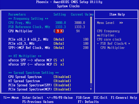
The deceptively-named System Clocks BIOS menu provides only PCI-Express and HyperTransport Interconnect frequency adjustments, otherwise focusing on bus multipliers.

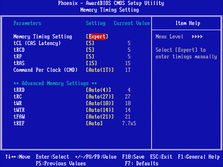
FSB and Memory clock speeds are found within the FSB & Memory Config menu. This is also where the memory timing sub-menu link appears.
Memory timings are adjustable to all reasonable settings, allowing top performance at any reasonable memory speed.

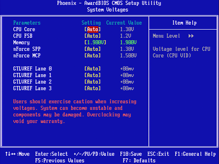
Voltage settings are a little more conservative, but broad enough to take most hardware to its limit.
Get Tom's Hardware's best news and in-depth reviews, straight to your inbox.
-
Crashman This was ALL OF THE AVAILABLE 790i Ultra SLI MOTHERBOARDS: Other graphics brands with NVIDIA reference boards INCLUDING EVGA are selling the same unit as XFX, even with the same BIOS (except for the boot logo). XFX was the only one who cared to send one.Reply -
giovanni86 Thats what i was going to say!!! Thank god. Well i guess i made the right choice. XFX 790i, exactly what i am going to buy in the coming month. Just need to save for it XD.Reply -
jaragon13 Who would pay four hundred dollars,when you can just buy a P45 for 100-150 dollars which has roughly the same real world experience as an X48 or 790I?Reply
Nah,I'd rather buy better and more reliable parts-such as power supply,processor,GRAPHICS CARD,and maybe go buy a rifle :P -
kitsilencer $400 for a motherboard? What the hell is wrong with the X48 Express that people would rather consider buying a 790i? And it can't be because of SLI. Makes more sense to buy the X48 and Crossfire.Reply -
Crashman jaragon13Who would pay four hundred dollars,when you can just buy a P45 for 100-150 dollars which has roughly the same real world experience as an X48 or 790I?Nah,I'd rather buy better and more reliable parts-such as power supply,processor,GRAPHICS CARD,and maybe go buy a rifleReply
If you want SLI you're going to need an SLI motherboard. The article specifically stated that the reference design motherboard was almost as good in many ways as the winning board, but far cheaper.
The site only has two awards, one is for top value and the other is for "best of the best". It's hard to award a $350 motherboard for top value, but it's not so difficult awarding the "best of the best" even if the price is outrageous -
Crashman kitsilencer$400 for a motherboard? What the hell is wrong with the X48 Express that people would rather consider buying a 790i? And it can't be because of SLI. Makes more sense to buy the X48 and Crossfire.Reply
It does! Well, sorta. If you want the absolute fastest rig on the planet, you're going to need at least two, possibly three, GTX280's. But if you can wait a few days or maybe a couple weeks, you might be surprised at how well a Crossfire set of HD4870X2's can perform using an X48 motherboard. -
jaragon13 My point is that,even though you could theoritically have 3/4 GPU's all at once,you won't get nearly as much performance as you'd want.A simple 750I or P45 chipset will do nearly the same job.Reply -
zer00000 It is a foxconn board i bet.I just read a review elsewhere with same stuff except it had an x48 chipset."All manner of goodies are bundled with the Black Ops: a 120MM fan, a plastic dry ice cooling pot for the Northbridge, and a Plexiglas "benching table" for open-air use."Reply

