790i Ultra SLI Motherboards Compared
BIOS and Overclocking
| FSB Frequency | 100 - 625 MHz (1 MHz) |
| Clock Multiplier Adjustment | Yes |
| DRAM Linked Ratios | Automatic Only |
| DRAM Unlinked Data Rate | 400 - 2500 MHz Data Rate |
| PCIe Clock | 100 - 200 MHz (1 MHz) |
| CPU Vcore | Stock to +0.78750 Volts (0.0125 Volts) |
| CPU FSB Voltage | - |
| Northbridge (SPP) | 1.200 - 1.600 Volts (0.025 Volts) |
| Southbridge (MCP) | 1.500 - 2.000 Volts (0.025 Volts) |
| DRAM Voltage | 1.50 - 2.50 Volts (0.10 Volts) |
| CAS Latency Range | tCAS: 5-18; tRCD: 1-15; tRP: 1-15; tRAS: 1-63 |
The P7N2 Diamond from MSI provides a more than adequate adjustment range for every available setting, but a couple of settings are missing: DRAM Linked Ratio and CPU FSB voltage.

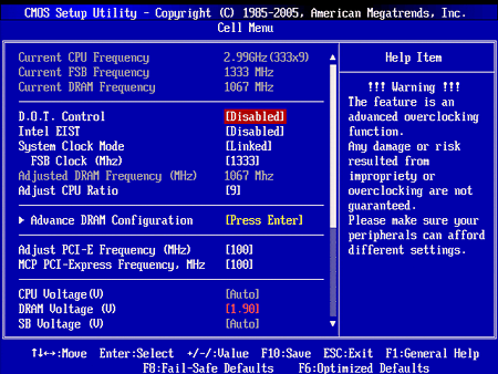
MSI’s Cell Menu puts most of the important controls on one long page, with CPU FSB, memory frequency, CPU multiplier, and bus speeds at the top.

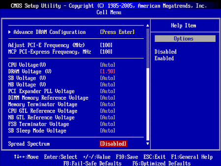
Scrolling down reveals the voltage settings, with a single CPU GTL Reference setting for all cores.

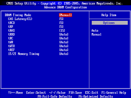
A submenu provides all the needed memory timings, with automatic adjustment available for every setting that the tuner doesn’t want to play with. Automatic settings for individual timings have long been standard on most brands, but this is a recent addition to the MSI BIOS.
Get Tom's Hardware's best news and in-depth reviews, straight to your inbox.
-
Crashman This was ALL OF THE AVAILABLE 790i Ultra SLI MOTHERBOARDS: Other graphics brands with NVIDIA reference boards INCLUDING EVGA are selling the same unit as XFX, even with the same BIOS (except for the boot logo). XFX was the only one who cared to send one.Reply -
giovanni86 Thats what i was going to say!!! Thank god. Well i guess i made the right choice. XFX 790i, exactly what i am going to buy in the coming month. Just need to save for it XD.Reply -
jaragon13 Who would pay four hundred dollars,when you can just buy a P45 for 100-150 dollars which has roughly the same real world experience as an X48 or 790I?Reply
Nah,I'd rather buy better and more reliable parts-such as power supply,processor,GRAPHICS CARD,and maybe go buy a rifle :P -
kitsilencer $400 for a motherboard? What the hell is wrong with the X48 Express that people would rather consider buying a 790i? And it can't be because of SLI. Makes more sense to buy the X48 and Crossfire.Reply -
Crashman jaragon13Who would pay four hundred dollars,when you can just buy a P45 for 100-150 dollars which has roughly the same real world experience as an X48 or 790I?Nah,I'd rather buy better and more reliable parts-such as power supply,processor,GRAPHICS CARD,and maybe go buy a rifleReply
If you want SLI you're going to need an SLI motherboard. The article specifically stated that the reference design motherboard was almost as good in many ways as the winning board, but far cheaper.
The site only has two awards, one is for top value and the other is for "best of the best". It's hard to award a $350 motherboard for top value, but it's not so difficult awarding the "best of the best" even if the price is outrageous -
Crashman kitsilencer$400 for a motherboard? What the hell is wrong with the X48 Express that people would rather consider buying a 790i? And it can't be because of SLI. Makes more sense to buy the X48 and Crossfire.Reply
It does! Well, sorta. If you want the absolute fastest rig on the planet, you're going to need at least two, possibly three, GTX280's. But if you can wait a few days or maybe a couple weeks, you might be surprised at how well a Crossfire set of HD4870X2's can perform using an X48 motherboard. -
jaragon13 My point is that,even though you could theoritically have 3/4 GPU's all at once,you won't get nearly as much performance as you'd want.A simple 750I or P45 chipset will do nearly the same job.Reply -
zer00000 It is a foxconn board i bet.I just read a review elsewhere with same stuff except it had an x48 chipset."All manner of goodies are bundled with the Black Ops: a 120MM fan, a plastic dry ice cooling pot for the Northbridge, and a Plexiglas "benching table" for open-air use."Reply
