 Join Tom’s Hardware today


Introduction
Yesterday (Aug 24, 1998) Intel announced three new processors, the Pentium II 450 and two new Celeron CPUs 'Celeron 300 A' and 'Celeron 333'. At the first look there's really nothing spectacular about those three new CPUs, it gives the impression as if Intel was simply cranking up the clock frequency.
The Major Difference Between the Old And the New Celeron - On-Die Full Speed 2nd Level Cache
The only thing that somehow catches attention is the little 'A' in the name of the new Celeron 300. So far there was a Celeron 266 and Celeron 300, both not exactly loved by the press or public. Those two 'old' Celerons are using the well known 'Deschutes' core that's also found in Pentium II and Pentium II Xeon processors. The Pentium II teams it up with two 'BSRAM' half speed 2nd level cache chips whilst the Xeon is running this core together with a full speed 'CSRAM' . The old Celeron however had to run the 'Deschutes' core without any 2nd level cache, thus making the product significantly cheaper than the two brothers whilst lowering the office application performance compared to Pentium II and Xeon significantly too. The 3D gaming performance of the old Celeron however was pretty impressive, making this CPU an excellent and cheap multi media solution for home users. Another big advantage of the 'cacheless' Celeron is its great usefulness for overclockers. Celerons running at 400 MHz in BX boards are a powerful and pretty inexpensive solution for people who don't fear overclocking and who are planning a future upgrade to a 100 MHz Pentium II CPU for the same motherboard.
The Old Celeron Is Almost Dead - Long Live The New Celeron!
Now what's the story about the 'A' and why is the new Celeron 333 unexpectedly different to a Celeron 266 or 300 that's simply running at 333 MHz? Well, first of all I would like to take the opportunity and congratulate Intel for the craziest marketing strategy I've ever come across. Releasing a product with a new name that gets pretty bad press and then launching a product with the same name that's significantly better is pretty much the opposite to what any other company has ever done or would ever do in the future. There is still a huge number of users out there who combine 'bad performance' with the name 'Celeron', generated by a vast amount of publications who only looked at office performance, ignoring the 3D and FPU performance at the same time. It seems as if Intel is very much depending on the press for letting the people know that the new Celeron is completely different. For the sake of my readership I won't disappoint Intel's expectations this time.
128 kB On-Die Full Speed 2nd Level Cache Makes the Difference
The new Celeron is indeed a whole lot different to its predecessor. The Celeron 300 A and the Celeron 333 comes now with an internal on-die 2nd level cache of 128 kB, which is even running at CPU clock frequency and thus faster than the 2nd level cache of a Pentium II running at only half the CPU clock frequency. This accelerates the new Celerons to a speed that's virtually identical to the speed of Pentium II CPUs at the same clock speed. Office applications, 3D games and even 3D rendering programs do hardly make any difference between 512 kB 2nd level cache running at half the CPU clock or 128 kB 2nd level cache running at CPU clock. There may be some software that takes particular advantage of the larger L2 cache of the Pentium II but at the same time there may be software that takes advantage of the faster L2 cache of the new Celerons.
Intel First On The Market With On-Die L2 Cache
The 'Mendocino' core used in the new Celeron CPUs comes with on-die L2 cache. This means that the L2 cache is on the same piece of silicon as the CPU core is. This is different to the Pentium II and Xeon, which both have their L2 cache modules outside the CPU chip. It's even different to the good old Pentium Pro, which had its L2 cache in the same package or chip, but inside the Pentium Pro there were two pieces of silicon put together. Since the CPU cores got shrunk to .25 micron, a 2nd level cache of 128 kB doesn't need a lot of space and can easily fit onto a CPU core, thus keeping the costs low. AMD and IDT announced the same plan about 10 months ago for their '+' successors of K6-2 and WinChip C6. Intel didn't announce anything like that at Microprocessor Forum last year, they simply did it, and they came out first as well.
The New Celeron - Still Overclocker No.1 s
Many of my experienced readers feared that the times of easily overclocking a Celeron will be over as soon as the on-die 2nd level cache will be included into it. My experiences with 'Mendocino' showed that this fear is not justified. As a matter of fact it blew me away when I saw that a Celeron 333 running at 450 MHz was even beating no less than the brand new and also just announced Pentium II 450. I only wish that Intel would drop the annoying restriction of the CPU multipliers. It only took a few weeks after my 'B21-article' and Intel shipped Celerons that would only run with the specified multiplier. The Celeron 266 was restricted to x4, thus running at 400 MHz and only 400 MHz when supercharged with 100 MHz FSB. The Celeron 300 coming with a x4.5 multiplier was in many cases not up to the 450 MHz it would have to reach at 100 MHz FSB. I am expecting the same problem with the new Celeron 300 A and Celeron 333. The more interesting product will again be the slower one, since the Celeron 300 'A' will most likely do 450 MHz and offer the speed of a Pentium II 450 for less than a third of its price. The Celeron 333 would have to be able to run at 500 MHz, which is pretty unlikely. I wonder why Intel does this multiplier restriction.
Intel's Policy - Fighting Counterfeits Or Fighting Overclockers?
The usual answer you get from Intel is that they want to avoid some criminals selling fake CPUs. "Intel hasn't got anything against people who like overclocking their chip, we just want to avoid fraud." I am asking why Intel is restricting lower multipliers as well then? Are they afraid of the bad gangster who will sell a Celeron 333 as a Celeron 300 A? There aren't any Celeron CPUs for 100 MHz FSB available, so the risk of a fake Celeron 400 or 450 is zero as well. Now Intel may say that the Celeron will do 100 MHz FSB in the future, which is why they don't even want to allow lower multiplier settings. Then I may ask why they cannot put a few a readable registers onto the CPU core, which could be checked by a CPUID program, thus marking each CPU for its official clock speed and finally making counterfeits impossible. We want to be honest, Intel doesn't want overclocking, they seem to hate it and they try whatever they can to make the life of overclockers harder, whilst not giving the slightest damn about a sensible strategy that would avoid counterfeits at the same time. I am not the first to demand software marking inside the chip, but I do also demand that Intel drops its petty attacks against overclockers unless Intel officially admits that they highly disapprove overclocking and will do the best against it. Basta, let's put the cards on the table guys!
What Do the new CPUs Look Like?
The new Celerons are not that easy to recognize. The difference to the Celerons without 2nd level cache is merely a different size of the metal cap that covers the CPU core. The old Celerons only host the .25 micron die underneath it, the new Celerons need some additional space for the on-die cache, making the die larger and thus the metal cap is larger as well.

The new Pentium II 450 looks just as it always did on the first look. The main difference is found inside. However, there's a little thing that makes the difference even from the outside. You may remember that the Pentium II 233 - 333 don't require any cooling of their 2nd level chips, thus the 'T-plate' that covers the chips at the side where the heat sink is connected to the cartridge is simply plain. The Pentium II 350 and 400 has two notches in the T-plate, assuring close contact and thus proper cooling for the two 2nd level chips inside the cartridge. Pentium II 450 is different. Inside you'll find a new package for the CPU core, that doesn't come with a metal cap covering the silicon chip anymore, but attaching the die directly to the T-plate. You'll also find that the two L2 cache chips are at the same side of the CPU core, not on each side as in the previous Pentium II models. The T-plate of the Pentium II 450 has thus only got one longer notch that ensures the contact to both L2 cache chips. Looking at the T-plate will straight away show if it is a Pentium II 450 or not. This is of course only valid until Intel starts building all 100 MHz FSB Pentium II CPUs this way.

The new Pentium II 450 has a completely new PCB layout, the core package is different and it is using 4.4 ns L2 cache chips from Samsung.

The T-plate makes the difference .. at least until it will be removed completely in SECC2.
A Word About The Pentium II Overdrive For Socket 8
Intel's announcement of the long, long, long awaited Pentium II Overdrive CPU came as a complete surprise to me. No word about it in the road map and also no information from Intel's spokesmen were the reasons why I couldn't believe my eyes when I read Intel's announcement. However, I don't seem to be the only one who's surprised. After receiving two samples of this PII OVD 333 I had to find out that none of my Socket 8 boards would recognize it properly. This is no big miracle, since the BIOSes of those motherboards are at least one year old now. I browsed the websites of the motherboard makers, but there was no word about the new Overdrive CPU and certainly not the sight of a new BIOS. So far I could only run the new chip in an old Abit PS6 board, but this board initializes only 256 kB of the 512 kB full speed L2 cache of the PII OVD. The performance was identical to PII 333 performance, but I guess we want to see results of a chip that runs as it's supposed to, with all it's L2 cache enabled. Abit's answer to my request for a new BIOS was "we don't sell this product anymore". Wow, thank you! I guess there's hardly any motherboard maker that sells Socket 8 boards anymore, but that doesn't mean that there's not a lot of people who still use it. So far about help from Abit. Tyan is still trying their luck on supplying me with a working BIOS for their excellent Socket 8 boards, but so far I'm still waiting. They told me they haven't even got a PII OVD to try the BIOS themselves. Well, looks like Intel took ages for supplying us with this chip and now there's no platform that supports it. This is not very Intel-like, they usually kick the butts of the motherboard makers for shipping the latest BIOS. Anyway, I'm still waiting to finally run the Mini-Xeon once there's a working BIOS available.
Benchmark Setup
- Slot 1 System:
- Asus P2B motherboard with Intel 440BX chipset
- 2x 64 MB LGS PC100 SDRAM DIMM with 7ns chips
- Adaptec 2940UW SCSI host adapter
- IBM DGVS 09U ultra SCSI hard drive, 10,000 RPM drive
- NVIDIA RIVA 128 AGP graphics card, driver 1.50H for Windows98 and Windows NT
- 3Dfx Voodoo2 12 MB 3D accelerator card, driver 4.10.01.0094-2.16
- Operating System Windows 98 4.10.1998
- Operating System Windows NT4 SP3
- Resolution 1024x768, 16 bit color, 85 Hz refresh rate
- Super7 System:
- Asus P5A motherboard with ALi Aladdin V chipset, rev. E
- 2x 64 MB LGS PC100 SDRAM DIMM with 7ns chips
- Adaptec 2940UW SCSI host adapter
- IBM DGVS 09U ultra SCSI hard drive, 10,000 RPM drive
- NVIDIA RIVA 128 AGP graphics card, driver 1.50H for Windows98 and Windows NT
- 3Dfx Voodoo2 12 MB 3D accelerator card, driver 4.10.01.0094-2.16
- Operating System Windows 98 4.10.1998
- Operating System Windows NT4 SP3
- Resolution 1024x768, 16 bit color, 85 Hz refresh rate
Office Performance Windows 98
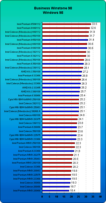
You can see how well the new Celeron with Mendocino core is doing, leaving the old Celeron far behind it. Overclocked to 450 MHz it's even a tad faster than a Pentium II 450, which I consider as pretty impressive. AMD's K6-2 is also doing pretty well, scoring very close to a Pentium II at the same clock speed. The new Asus P5A is a platform which makes the K6-2 real fun. As I have said in my K6-2 article, all it takes for the K6-2 to be a winner is a reliable Super7 platform. Asus provides an excellent example for that. Please also note how well the Cyrix MII or IBM 6x86 is scoring. However please realize also that the P-rating is close to a merely misleading kind of naming. A MII 333 scores far from a Pentium II 333 or an AMD K6-2 333, unless you are running your system with unrealistically small amounts of RAM, as e.g. done in those nice benchmarks published by Cyrix and IBM. This is why I did not list the P-rating but the real clock rates instead.