Nvidia’s GF100: Graphics Architecture Previewed, Still No Benchmarks
Get Tom's Hardware's best news and in-depth reviews, straight to your inbox.
You are now subscribed
Your newsletter sign-up was successful
GF100: The Chip Based On Fermi
The dichotomy that is AMD’s and Nvidia’s respective design principles persists in 2010.
The former stands by its “sweet spot” strategy, whereby a reasonably-sized GPU (if you can call a 2.15 billion transistor chip reasonable) serves to address what we’d call the high-end market, while derivatives cover the price segments below. Addressing the more demanding enthusiast community involves multi-GPU configurations—this generation’s example is the dual-GPU Radeon HD 5970.
Meanwhile, Nvidia has another behemoth on its hands. Though the two companies almost certainly count transistors differently, GF100 is said to consist of more than three billion of them, up from the GT200’s 1.4 billion. There’s no word yet how Nvidia plans to implement lower-cost versions of its Fermi architecture—all of the details being released now center on one specific chip—but as you’ll see, the design is deliberately modular. So, whereas all of the GeForce GTX 200-series boards employed one (expensive) GPU, there’s a better chance that this time we’ll see Nvidia do some cutting on lower-end versions.
As with ATI’s Radeon HD 5000-series cards, Nvidia employs TSMC’s 40nm manufacturing process, which has thus far struggled to reach the yield levels needed for AMD to meet its demand. It’ll be interesting to see if the fab’s teething pains affect Nvidia similarly.
And given Nvidia’s cautionary note on power, it’s a fairly safe bet that dual-GPU versions a la GeForce GTX 295 will make way for dual-card SLI configurations instead. Not that we expect Nvidia to need a card with two GF100s on-board. Should the company achieve ~2x the performance of GeForce GTX 285 in today’s games (and it’d appear that, given improvements to texturing/AA, GF100 will see scenarios in excess of a 2x boost), it’ll already be competing against Radeon HD 5970 using one graphics processor.
The Building Blocks
So, why exactly might we suspect GF100 of outperforming its predecessor by such a compelling margin? It’s largely a matter of comparing architectures. Fortunately, the GF100 design is derived from GT200, which itself was derived from the almost-infamous G80/G92. If you’re already familiar with Nvidia’s previous-generation designs, understanding its latest should be somewhat straightforward.
Get Tom's Hardware's best news and in-depth reviews, straight to your inbox.
The fundamental building block remains the stream processor, marketed now as a CUDA core. GF100 boasts 512 of these CUDA cores versus GT200’s 240. Thus, clock for clock, we’re looking at the potential for 2.13x the performance of GeForce GTX 285, assuming no other optimizations. However, Nvidia was aware of GT200’s weaknesses in designing GT100, and it claims those have been addressed here with a bit of architectural shuffling. In reality, Nvidia says it’s seeing performance in today’s titles roughly two times higher than GT200 with 8xAA enabled.
The GPC
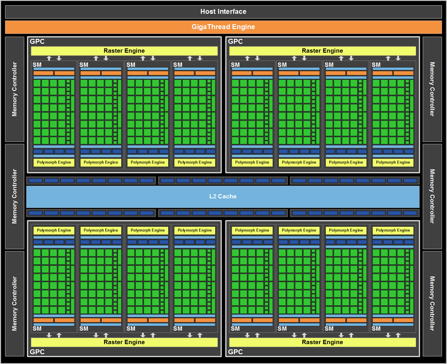
GT200 sports 10 of what Nvidia calls Texture Processing Clusters (TPCs), each armed with three Streaming Multiprocessors (consisting of eight stream processors and eight texture address/filtering units). That fundamental organization evolves this time around to include a more elegant collection of resources, from the fixed-function raster engine to as many as four of those Streaming Multiprocessors.
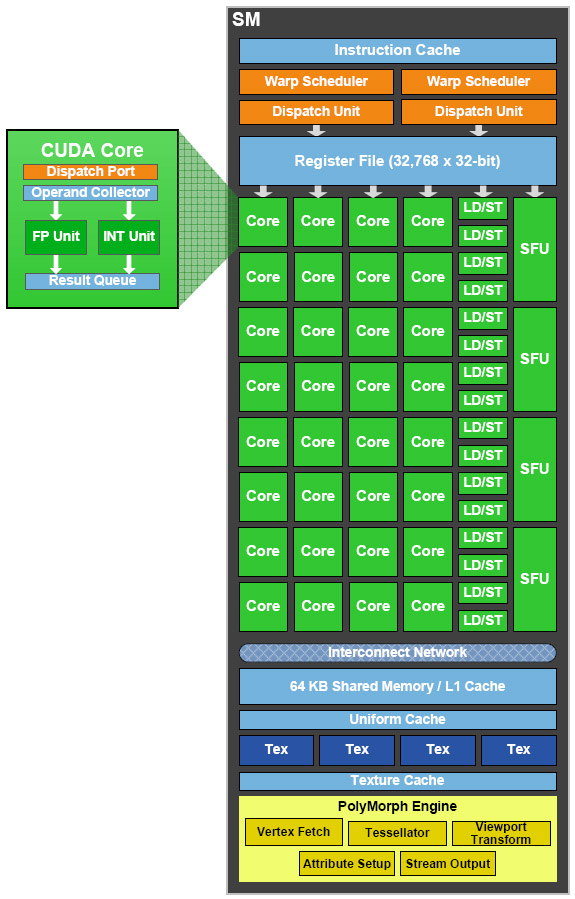
These blocks of logic are divided into Graphics Processing Clusters (GPCs), displacing the TPC concept by integrating functionality that previously existed outside the TPC. Now, one GPC is armed with its own raster engine interfacing with up to four SMs, each SM sporting 32 CUDA cores and four dedicated texture units (along with what Nvidia claims as dual schedulers/dispatchers and 64KB of configurable cache/shared memory). GF100, in its fully-operational Death Star configuration, is equipped with four GPCs.
By the numbers, GT200 actually has more texturing units than GF100 (eight per TPC, up to 10 TPCs per GPU versus four texturing units per SM, with up to 16 SMs). However, the focus here is on augmented efficiency: each texture unit computes one address and fetches four samples per clock. As a result, GF100 achieves higher real-world performance, according to Nvidia.
Scheduling Via GigaThread
The GPCs are fed by Nvidia’s GigaThread Engine. Made kid-friendly by Nvidia’s marketing team, the engine is GF100’s scheduler, responsible for assigning work to each of the chip’s 16 SMs. Yet it establishes itself as a significant component of the Fermi architecture due to its ability to create and dispatch thread blocks in parallel, rather than the one-kernel-at-a-time approach taken before.
Of course, the GigaThread engine fetches its data from the frame buffer. At first blush, the six 64-bit controllers (totaling 384-bits) seems narrower than GT200’s eight x 64-bit (512-bit total) configuration. However, Nvidia is utilizing GDDR5 this time around, yielding a substantial bandwidth increase, despite the less-complex interface. Assuming the same 1,200 MHz DRAMs AMD is using on its Radeon HD 5870, a GF100-based card would have access to 230.4 GB/s of throughput versus the Radeon’s 153.6 GB/s.
ROP Performance
The back-end of GF100 is organized into six ROP partitions able to output eight 32-bit integer pixels at a time. This compares favorably to GT200’s eight blocks capable of four pixels per clock. Nvidia maintains one 64-bit memory controller per block, but realizes an overall increase from 32 pixels per clock to 48. Perhaps you noticed that, in our Radeon HD 5870 coverage, improvements to ATI’s anti-aliasing performance over its previous-generation hardware. Meanwhile, the GT200-based GeForce GTX 285 took a more substantial hit as you cranked up AA.
This is another area where Nvidia sought to improve with GF100. If you own a card like ATI’s Radeon HD 5870 or are planning to buy something based on GF100, and are running on one display, then you’re enabling whatever detail settings you can in order to utilize the GPU’s massive performance. To this end, GF100 supports a new 32x coverage sampling anti-aliasing (CSAA) mode that Nvidia demonstrated smoothing out banding issues in foliage generated using alpha textured billboards in Age of Conan. And as a result of its optimizations, Nvidia is claiming a less-than 10% performance hit in going from 8x multi-sampling to 32x CSAA.
Current page: GF100: The Chip Based On Fermi
Prev Page Introduction Next Page Why Re-Organize GF100? One Word: Geometry-
randomizer GF100 is entering the ranks of Duke Nukem Forever. We keep seeing little glimpses but the real thing might as well not exist.Reply -
duckmanx88 dingumfOh look, no benchmarks.Reply
wth is he supposed to benchmark? nothing has been released it's just an article giving us details on what we can expect within the next two months. -
decembermouse I feel like you left some info out, whether you just never read it or didn't mention it for fear of casting doubts on GF100... I've heard (and this isn't proven) that they had to remove some shaders and weren't able to reach their target clocks even with this revision (heard the last one didn't cut the mustard which is why they're hurrying the new one along and why we have to wait till March). Also, be careful about sounding too partisan with Nvidia before we have more concrete info on this.Reply
And yes, it does matter that AMD got DX11 hardware out the gate first. Somehow, when Nvidia wins at something, whether that's being first with a technology, having the fastest card on the market, or a neato feature like Physx, it's a huge deal, but when AMD has a win, it's 'calm down people, let's not get excited, it's no big deal.' The market and public opinion, and I believe even worth of the company have all been significantly boosted by their DX11 hardware. It is a big deal. And it'll be a big deal when GF100 is faster than the 5970 too, but they are late. I believe it'll be April before we'll realistically be able to buy these without having to F5 Newegg every 10 seconds for a week, and in these months that AMD has been the only DX11 player, well, a lot of people don't want to wait that long for what might be the next best thing... all I'm trying to say is let's try not to spin things so one company sounds better. It makes me sad when I see fanboyism, whether for AMD, Intel, Nvidia, whoever, on such a high-profile review site. -
megamanx00 Well, not much new here. I wouldn't really be surprised if the 2x performance increase over the GTX285 was a reality. Still, the question is if this new card will be able to maintain as sizable a performance lead in DX11 games when Developers have been working with ATI hardware. If this GPU is as expensive to produce as rumored will nVidia be able to cope with an AMD price drop to counter them?Reply
I hope that 5850s on shorter PCBs come out around the time of the GF100 so they can drop to a price where I can afford to buy one ^_^ -
cangelini dingumfOh look, no benchmarks.Reply
*Specifically* mentioned in the title of the story, just to avoid that comment =) -
randomizer cangelini*Specifically* mentioned in the title of the story, just to avoid that comment =)You just can't win :lol:Reply -
WINTERLORD great article. im wondering though just for clarifacation, nvidia is going to look better then ati?Reply -
tacoslave Even though im a RED fan im excited because its a win win for me either way. If amd wins than im proud of them but if nvidia wins than that means price drops!!! And since they usually charge more than ati for a little performance increase than ill probably get a 5970 for 500 or less (hopefully). Anyone remember the gtx280 launch?Reply


