Intel's New Pentium 4 Processor
Get Tom's Hardware's best news and in-depth reviews, straight to your inbox.
You are now subscribed
Your newsletter sign-up was successful
Advanced Transfer Cache
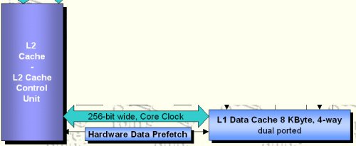
The next thing that (most of) the data has to pass is Pentium 4's on-die L2-cache. Intel calls it 'Advanced Transfer Cache' since the days of Pentium III 'Coppermine' . With 256 kB its size is identical to the L2-cache of Pentium III and both are 8-way associative as well. This is however where the similarities end. Pentium 4's L2-cache is using 128-Byte cache lines, which are divided in two 64-Byte pieces. When it fetches data from the system (main memory, AGP, PCI, ...) it reads at least 64 Bytes in one go, which ensures great performace for burst transfers, especially when talking to RDRAM, but is rather bad if only one Byte out of that 64 is actually required. The same is obviously valid for write operations in case the cache line has become 'dirty', meaning that the cache data has been altered and therefore needs to be written back to the system (memory, AGP, PCI, ...). The read latency of Pentium 4's L2-cache is 7 clocks, its connection to the core is 256 bit wide and obviously clocked at core clock. After doing the math we get to an impressive data bandwidth between L2-cache and core of 44.8 GB/s for Pentium 4 @ 1.4 GHz and 48 GB/s for Pentium 4 at 1.5 GHz.
Pentium 4's L1 Cache
After the discussion of the L2 cache it wouldn't be more than logical to move over to the L1 cache. This is what we will do, but not without a special remark. While Pentium III is equipped with a 16 kB L1 cache for instructions and a 16 kB L1 cache for data, there is only an 8 kB small data L1 cache in Pentium 4, while a pretty nifty feature called 'Execution Trace Cache', which I'll discuss in the next paragraph, replaces the L1 instruction cache of Pentium III.
Intel was probably forced to reduce the size of the L1 data cache down to only 8 kB, which is half the size of Pentium III's L1 data cache and only an eighth (!!!) of Athlon's, to enable its extremely low latency of only 2 clock cycles. It results in an overall read latency of less than half of Pentium III's L1 data cache already in the Pentium 4 at 1.4 GHz, but the small size of Pentium 4's L1 data cache may be one reason for the performance flaws we will see when we get to the benchmark results.
The L1 data cache of Pentium 4 is 4-way set associative and uses 64-Byte cache-lines. The dual-port architecture allows one load and one store operation per clock.
Hardware Prefetch
Intel has added another nifty feature that I want to bring to your attention in the L1/L2 cache context. If you think of the Pentium III launch in February 1999, you might remember Intel's introduction of the 'streaming' SIMD Extensions. The 'streaming' bit of 'SSE' is actually represented by the prefetch-instructions of Pentium III, which enable software to load data into the caches before it is requested by the processor core.
Those instructions still exist in Pentium 4's instruction set, but with the new hardware prefetch feature of Pentium 4 a lot of this is done automatically. This new unit is able to recognize data access patterns of the software executed by Pentium 4, so that it 'guesses' which data will be needed next and 'pre-fetches' it into the cache.
The procedure might sound familiar to you from the complex hard drive cache algorithms and you might also be aware how much this can speed up hard disk accesses under certain circumstances. Pentium 4's hardware prefetch is probably able to significantly accelerate the execution of software that is using a lot of large data arrays.
Get Tom's Hardware's best news and in-depth reviews, straight to your inbox.
Entering The Execution Pipeline - Pentium 4's Trace Cache
Our code has now passed the system bus, L1 and L2-cache, so that it's finally time to enter the execution path of Pentium 4. You remember that Pentium 4 is not using an L1 instruction cache, but a much niftier thing instead. Let me first explain what is bad about an L1 instruction cache.
With Pentium III or Athlon, who both have an L1 instruction cache, code is fetched by this cache and stored until it's about time to enter the execution path. This is done by code entering the decoder unit, which e.g. in case of Athlon consists of 3 'direct path' and 3 'vector path' decoders, which alternatively produce the 'OPs' (as explained above) that can get executed by the execution units of the processor. This situation has a few glitches. First of all, some x86-instructions are rather complex, taking a lot of time to be decoded by the slow or 'vector path' decoders. In the worst case all decoder units are busy decoding complex instructions, thus stalling the execution pipeline of the processor. Another problem is the fact that x86-instructions that are supposed to be executed repeatedly (e.g. in small loops) need to be decoded each time they enter the execution path, thus wasting a lot of time. Software branches are another wasteful situation for a processor with L1 instruction cache that starts its pipeline at the decoder level.
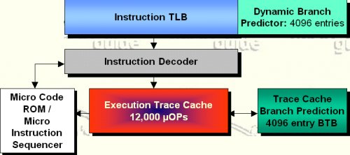
Pentium 4's fancy Execution Trace Cache does not suffer from the above-described problems. Once you understood it, the idea of the trace cache is actually rather simple, but it takes quite a bit more silicon resources and design skill to replace the good old L1 instruction cache with something like Pentium 4's trace cache. Basically, the 'Execution Trace Cache' is nothing but a L1 instruction cache that lies BEHIND the decoders. Obviously it's quite bit more complex, but once you understood this basic fact you start to realize the benefits of the trace cache.
Current page: Advanced Transfer Cache
Prev Page What's Behind NetBurst? Next Page Entering The Execution Pipeline - Pentium 4's Trace Cache, Continued-
ta152h utahraptorI just don't see this Rambus lasting that long. I think the future lies in DDR.Reply
I think the Pentium 4 will not last past 2006.

