ATI Radeon HD 4890: Playing To Win Or Played Again?
Building A Radeon HD 4890
Architecturally, the RV790 graphics processor is identical to RV770. The vital specs haven’t changed one bit. It’s still a 55 nm component, though transistor count is up just slightly to approximately 959 million transistors (from 956 million). The GPU is still made up of 800 stream processors, 40 texture units, and 16 ROPs. It still sports a 1 GB GDDR5 frame buffer on a 256-bit memory bus, too.
Where it differs most is clock speed—on its core and memory bus. Stock Radeon HD 4870s employed a 750 MHz engine and quad data rate memory running at 900 MHz. This new offering cruises at 850 MHz with 975 MHz GDDR5 memory.
In order to get those elevated frequencies, ATI had to do some work to the GPU’s core. In short, the RV770 consistently had issues clocking beyond a certain point—a fact that was evident in many of our System Builder Marathon overclocking attempts, which generally fell short at the same frequency range.
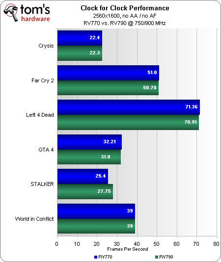
The company’s engineers went in looking for slow electrical paths and re-wired them in such a way that they wouldn’t inhibit faster frequencies. Physically, the GPU is fractions of a millimeter larger due to additional capacitors that clean up power to the chip. But it remains the same ol’ design popularized mid-2008. As you can see from the table above, clock-for-clock RV770 and RV790 perform nearly-identically clock-for-clock.
| Header Cell - Column 0 | Radeon HD 4870 X2 | Radeon HD 4890 | Radeon HD 4870 | GeForce GTX 285 | GeForce GTX 260 Core 216 |
|---|---|---|---|---|---|
| Manufacturing Process | 55 nm TSMC | 55 nm TSMC | 55 nm TSMC | 55 nm TSMC | 55 nm TSMC |
| SPs | 1,600 (2 x 800) | 800 | 800 | 240 | 216 |
| Core Clock | 750 MHz | 850 MHz | 750 MHz | 648 MHz | 576 MHz |
| Shader Clock | 750 MHz | 850 MHz | 750 MHz | 1,476 MHz | 1,242 MHz |
| Memory Clock | 900 MHz GDDR5 | 975 MHz GDDR5 | 900 MHz GDDR5 | 1,242 MHz GDDR3 | 999 MHz GDDR3 |
| Frame Buffer | 2 x 1 GB | 1 GB | 1 GB / 512 MB | 1 GB | 896 MB |
| Memory Bus Width | 2 x 256-bit | 256-bit | 256-bit | 512-bit | 448-bit |
| ROPs | 2 x 16 | 16 | 16 | 32 | 28 |
| Price | $400 | $249 | ~$180 | $340 | ~$180 |
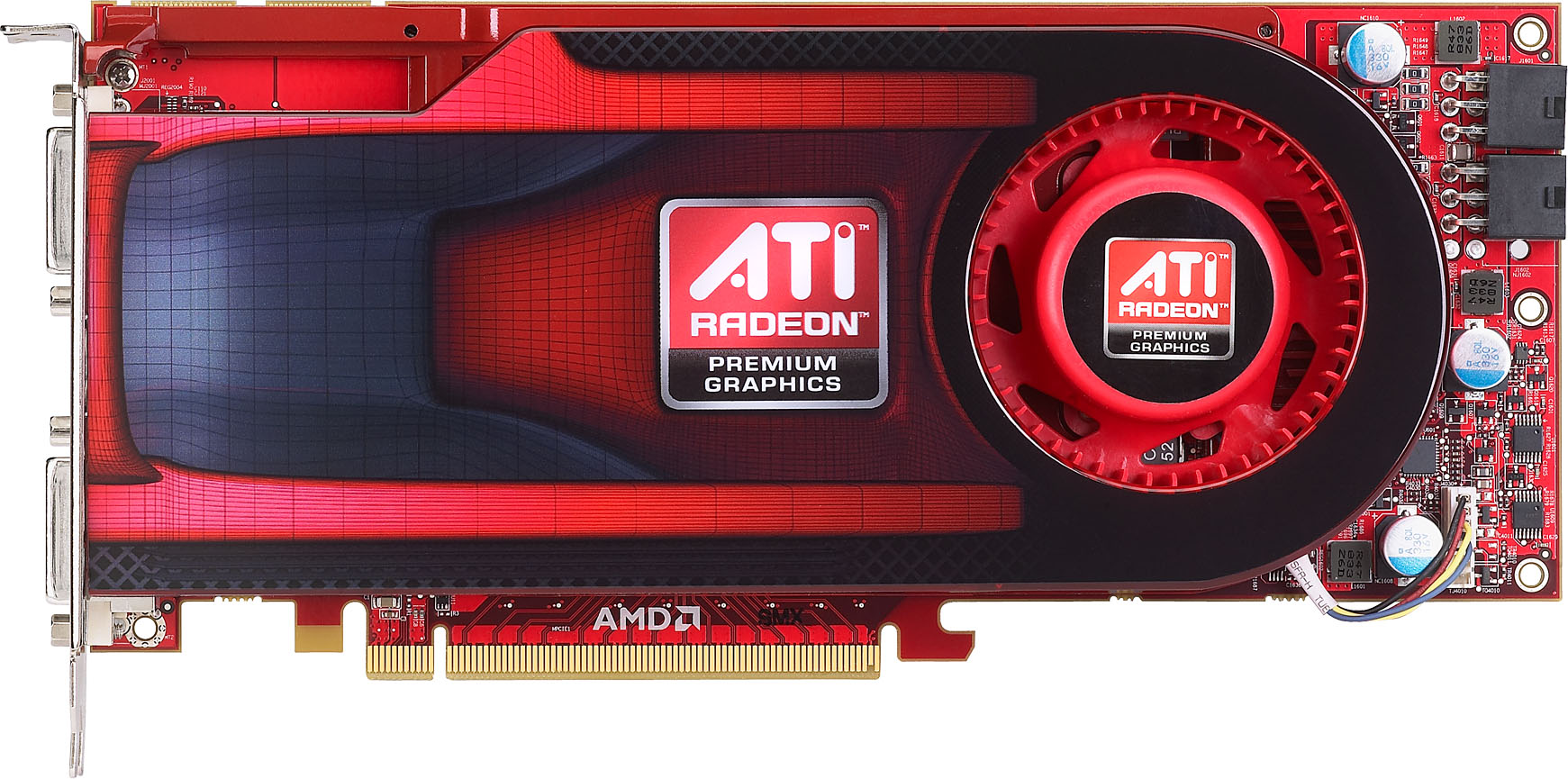
Not surprisingly, the 4890 card itself is easily mistaken for a Radeon HD 4870. They’re the same length; they both employ dual-slot coolers and the same dual-DVI plus video output configuration. Subtle differences set the two cards apart, giving away the fact that these two boards are indeed based on different GPUs. And despite the slight increase in load power consumption as a result of the 4890’s higher clock speed, ATI still gets away arming the card with two six-pin auxiliary power connectors.
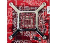
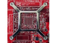
As of right now, ATI doesn’t have plans for a Radeon HD 4890 X2 variant, as it likely wouldn’t offer much more than a Radeon HD 4870 X2. And the chip’s extra full-load power consumption would create additional heat that’d need to be cooled.
Overclocking
Get Tom's Hardware's best news and in-depth reviews, straight to your inbox.
The principal benefit from moving from HD 4870 to HD 4890 would, in our minds, be overclocking headroom. Stock-to-stock, you’re looking at a 100 MHz frequency increase. However, right out of the gate, ATI’s board partners will be shipping juiced models running a 50 MHz-faster core clock. According to AMD, the new GPU layout should be capable of going even faster than that.
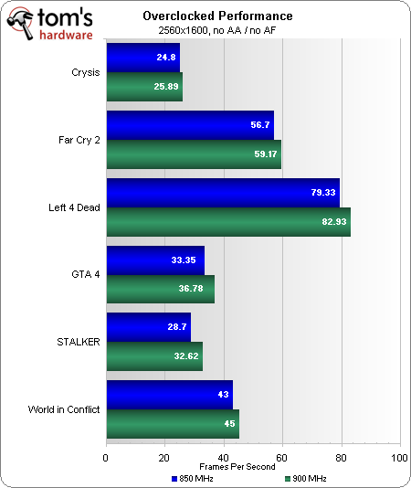
The driver’s Overdrive sub-routine now offers a maximum frequency of 1 GHz, suggesting ATI is fairly comfortable with its enthusiast customers running at that speed. Rather than push our card that high and run the risk of misrepresenting performance with a hand-picked sample, however, we ran our HIS Radeon HD 4890 Turbo sample at its stock 900/975 MHz speeds and compared it to the reference clocks ATI is officially launching.
Upping the core clocks to 900 MHz is good for gains between five and 10% at 2560x1600. One of these factory-overclocked boards undoubtedly enhances the value of ATI’s Radeon HD 4890 versus the 4870 1 GB. However, there will undoubtedly be an additional price premium over the reference cards, too, softening the worth of that extra performance to some degree.
Current page: Building A Radeon HD 4890
Prev Page Introduction Next Page The Relevance Of DirectX 10.1-
eklipz330 i usually don't bitch and moan about them not having enough test gpu's, but i'd really like to see that sapphire 2gb 4870 up there, seeing how its in the same price range as the 4890...Reply
any of these cards would suffice for me, 1680*1050 does save you a pretty penny -
ravenware http://firingsquad.com/hardware/ati_radeon_4890_nvidia_geforce_gtx_275/page4.aspReply
It seems to overclock well and outpaces the 275.
The stalker results seem odd from both review sites. But stalker is glitchy.
If priced right this should be a decent addition to the 4x series.
It holds its own against the 275 and in certain games the 285.
Perhaps sapphire will release a dual card.
The 4850x2 they released performed extremely well.
-
megamanx00 The 4850X2 is absent to compare to I see. Still nice to finally see a review of this thing. Nice gains over the 4870.Reply -
eklipz330 ReplyStalker: Clear Sky benchmarks are fairly new in our graphics card reviews, even if the game itself isn’t particularly fresh.Let us know what you think of this one in the comments section. At the very least, it’s a beautiful looking game.
any benchmark is welcome i suppose
too bad price goes up exponentially for minimal improvements... the 4890 will be about %50 more than the 4870 -
cangelini Both the 2 GB card and the 4850 X2 are exclusive to Sapphire, and neither has been sent over. Nevertheless, we'll be following up with SLI/CrossFire scores in the near future and I'll see if either of those two solutions might be lined up for that story.Reply -
eklipz330 cangelini, you are the man.Reply
just thought i'd let you know. this article was very well written, and you said everything i was thinking including the pricing. too bad you have to go to the other article to refer to gtx275 comparisons. regardless of that, gj -
cangelini Thanks Ek. Truth be told, both companies pulled their launches in, allowing about a week to get the testing/writing done. Usually that's pretty tight for one new launch. Two is a little rougher. But hopefully there was enough cross-linking between the pair to convey the right messages.Reply -
ifko_pifko I'll post it here as well as in the GTX275 review:Reply
Summing all the framerates is just nonsense. ;-) The games with higher fps will weigh more than the others.
