Snapdragon 810 Performance Preview
Qualcomm’s first 64-bit SoC is finally here, but swirling rumors about overheating and poor memory performance continue to smolder. Will the Snapdragon 810 burn up our benchmark charts or just go up in smoke?
Get Tom's Hardware's best news and in-depth reviews, straight to your inbox.
You are now subscribed
Your newsletter sign-up was successful
Architecture
Architecture
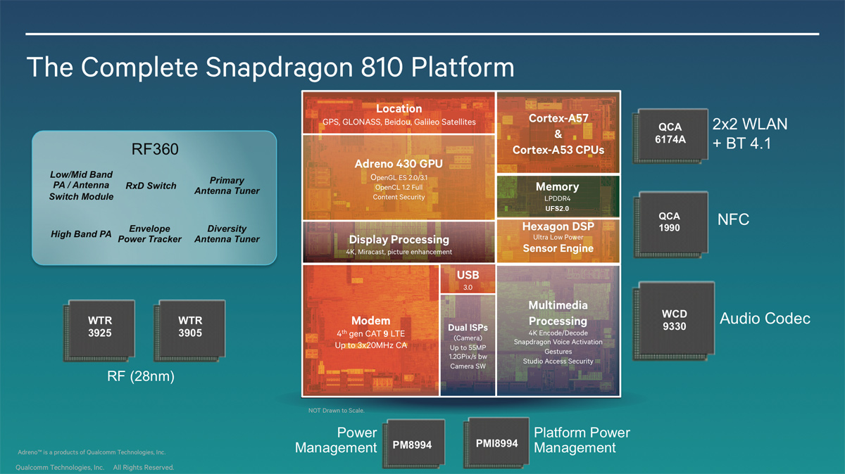
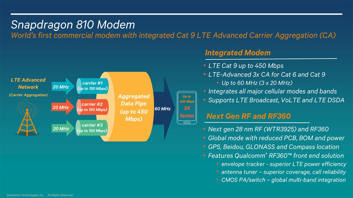
For Snapdragon 810, the big story is the move to a 64-bit CPU architecture. However, the 810 also contains an updated GPU, an all new memory interface, and a brand new Gobi modem. This last component is the 810’s biggest technological leap, supporting Category 9 LTE speeds up to 450 Mbps with carrier aggregation. While Snapdragon 805’s modem got voted off the SoC island, the 810 repatriates the modem, which should bring both power and cost savings.
| Qualcomm's Snapdragon 8xx Family | ||||
|---|---|---|---|---|
| Row 0 - Cell 0 | Snapdragon 810 | Snapdragon 805 | Snapdragon 801 | Snapdragon 800 |
| Manufacturing Process | 20nm | 28nm HPm | 28nm HPm | 28nm HPm |
| CPU | 4x ARM Cortex-A57 @ 2.0GHz + 4x ARM Cortex-A53 @ 1.5GHz (big.LITTLE) | 4x Qualcomm Krait 450 @ 2.65GHz | 4x Qualcomm Krait 400 up to 2.45GHz | 4x Qualcomm Krait 400 up to 2.26GHz |
| Architecture | ARMv8-A (32/64-bit) | ARMv7-A (32-bit) | ARMv7-A (32-bit) | ARMv7-A (32-bit) |
| GPU | Qualcomm Adreno 430 @ 600MHz | Qualcomm Adreno 420 @ 600MHz | Qualcomm Adreno 330 @ up to 578MHz | Qualcomm Adreno 330 @ 450MHz |
| Memory Interface | LPDDR4-1600 2x 32-bit (25.6GBps) | LPDDR3-800 2x 64-bit (25.6GBps) | LPDDR3-800/933 2x 32-bit (12.8/14.9GBps) | LPDDR3-800 2x 32-bit (12.8GBps) |
| Camera ISP | 14-bit dual ISPs (1.2GP/s throughput, image sensors up to 55MP) | 12-bit dual ISPs (1.2GP/s throughput, image sensors up to 55MP) | dual ISPs (930MP/s throughput, image sensors up to 21MP) | dual ISPs (640MP/s throughput, image sensors up to 21MP) |
| DSP | Hexagon V56 @ 800MHz | Hexagon V50 @ 800MHz | Hexagon V50 @ 800MHz | Hexagon V50 @ 680MHz |
| Integrated Modem | MDM9x??, LTE Cat 9, up to 450 Mbps | - | MDM9x25, LTE Cat 4, up to 150 Mbps | MDM9x25, LTE Cat 4, up to 150 Mbps |
CPU
The Snapdragon 810 moves away from Qualcomm’s custom Krait CPU architecture, instead following other SoC vendors like Marvell, MediaTek, and Nvidia in adopting stock 64-bit cores from ARM. Specifically, the 810 employs four Cortex-A57 and four Cortex-A53 cores in a big.LITTLE heterogeneous configuration, where all eight cores are available to the OS scheduler. The two CPU clusters are connected by ARM’s CCI-400 Cache Coherent Interconnect. Both of these CPUs are known quantities at this point, so we’ll just review the highlights.
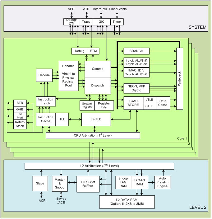
The Cortex-A57 is the successor to the Cortex-A15. Whereas the A15 was a new architecture, the A57 brings only minor revisions to the A15 design. It still has a speculative issue superscalar 15+ stage pipeline, where the first 12 stages (fetch/decode) are in-order and the final 3-12 stages (issue/execution) are out-of-order. IPC is also unchanged from the A15, decoding up to three, issuing up to eight, and retiring up to three (the eight pipelines have different lengths) instructions per cycle—half of what Apple’s A7 (presumably A8) and Nvidia’s Denver (it’s actually a 2- to 7-wide core depending on dynamic code optimization) can do. The instruction reorder buffer, which effects the level of instruction parallelism the core can achieve, holds up to 128 micro-ops, again the same as the A15, which is less than the 192 stored by Apple’s A7 (presumably A8) and Intel’s Haswell desktop architecture (while Denver lacks a hardware reorder buffer, its translation software performs reordering and looks across 1000+ instructions for parallelism). The L1 instruction cache grows to 48 KB (48-entry TLB) versus 32 KB for the A15, but keeps the same 32 KB data (32-entry TLB) cache. The L1 cache is backed by a shared L2 cache.
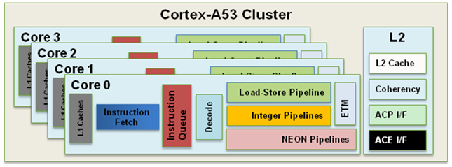
Article continues belowThe other CPU core in the big.LITTLE set is the Cortex-A53, which builds on the Cortex-A7 architecture. Where the A57 is a complex out-of-order core designed for high performance, the A53 is a very simple in-order core optimized for low power. It has a short 8-stage pipeline (the optional Advanced SIMD module, which Snapdragon 810 includes, uses 10 stages total and is required for performing floating-point operations) with symmetric dual-issue for most instructions. ARM claims that on the same process node the A53 delivers the same performance as the Cortex-A9.
Both the A57 and A53 share many low-level features with the CPUs they replace, but add support for the new 64-bit AArch64 architecture and A64 instruction set. The most obvious benefit of moving to 64-bit is being able to address more than 4GB of physical RAM, increasingly important for mobile devices where the CPU and GPU both share the same system RAM. The 32-bit A15 already uses Large Physical Address Extensions (LPAE), which map 32-bit virtual address spaces into a 40-bit physical address space with a 4 KB page resolution. This allows multiple apps to each see up to 4GB of memory at the same time, similar to how Windows programs worked on 32-bit x86. ARMv8-A alleviates memory address limitations by supporting 48-bits of both virtual and physical address space. Full 64-bit address spaces just aren’t necessary yet (x86-64 also uses 48-bit user space addressing) and limiting the address space simplifies the hardware and saves power. The new architecture also supports 64 KB page sizes in addition to the traditional 4 KB, which reduces page table walk from four to two levels when using a 42-bit address.
We likely won’t see smartphones and tablets with more than 4GB of RAM until at least 2016, but the move to 64-bit now offers other performance improvements. Registers are now 64-bits wide and there’s more of them; general purpose registers increase from 14 to 32 and SIMD/floating point registers increase from 16 to 32. The additional registers give compilers more room to perform loop unrolling and provides “improved scheduling options for the increasingly complex algorithms that are becoming common across various software codes,” according to ARM.
Rather than adapting the existing 32-bit decode table, ARM gave 64-bit instructions their own. Having two simple tables instead of one large, unwieldy table simplifies the hardware implementation and allows for easier branch prediction and other techniques for accelerating JIT compilers (JavaScript), useful for faster web browsing.
Get Tom's Hardware's best news and in-depth reviews, straight to your inbox.
ARM took the same approach to developing its 64-bit instruction set architecture (ISA). Rather than extending the A32 ISA, like AMD did with x86, ARM created a brand new, streamlined A64 ISA that further simplifies hardware implementation and lowers power consumption. For example, the load/store multiple instructions, which increased the memory system’s complexity, were removed along with some conditional instructions whose benefit couldn’t justify their power cost.
A64 also gives the advanced SIMD new capabilities to satisfy the IEEE754-2008 standard, including the ability for vectors to handle double precision floating point values and new number rounding instructions. The SIMD registers are also now 128-bits wide, up from 64-bits in AArch32.
Based on this information, will Snapdragon 810 offer better CPU performance than previous Snapdragon 80x SoCs? In general, and especially if running 64-bit code, the answer is yes. Krait 400/450 is basically a simplified version of the A15 optimized for low power and/or high clock frequencies. IPC is similar to A15/A57, with the same 3-wide front-end but one less execution port. Krait’s integer pipeline is also shorter, it has a much smaller instruction reorder buffer that only holds 40 micro-ops, and has smaller L1 caches. Having one less execution port and a smaller reorder buffer will definitely hurt overall throughput, although Krait’s shorter pipeline and higher clock speed will help it recover from a branch mispredict faster.
What about power consumption? All things being equal, the A57’s greater complexity translates to higher power draw. However, by racing to sleep, offloading tasks to the power efficient A53 cores, and being built on a smaller 20nm process should help mitigate this power penalty compared to Krait.
GPU
While we know quite a bit about the CPUs inside Snapdragon 810, we know next to nothing about its Adreno 430 GPU. Qualcomm has not shared any architectural details, just vague claims of 30 percent better performance and 20 percent lower power than the previous generation Adreno 420. Since the 420 saw a substantial architectural overhaul, it’s probably safe to assume that the 430 is a tweaked version of the 420.
Last year, the Adreno 420 added support for OpenGL ES 3.1 (plus Android Extension Pack), OpenCL 1.2, and DirectX 11 feature level 11_2, along with support for geometry shaders, dynamic hardware tessellation, and Adaptive Scalable Texture Compression (ASTC). All of these features carry over into the 430.
In our Snapdragon 805 preview, we noted that the large increase in memory bandwidth, along with Adreno 420’s larger texture and L2 caches, were likely feeding additional texture and shader units, a conclusion supported by benchmark results. With ample memory bandwidth and more die area available from the move to the smaller 20nm process, it’s likely Adreno 430 adds more shading resources.
One thing we noticed about devices running Snapdragon 805, like the Galaxy Note 4 and Nexus 6, is significant thermal throttling when playing games. In many cases, thermal throttling negates any performance benefit the 420 has over the older Adreno 330. The shift to a smaller process will help the 430 offset at least some of the power penalty from the (possible) increase in transistors—it’s likely Qualcomm made a few other power saving tweaks too—but I suspect thermal throttling will still be an issue for the 430, especially for all-plastic phones.
Memory
Snapdragon 805 accesses its LPDDR3-800 memory over a 64-bit dual-channel (128-bit total) bus yielding 25.6GBps of memory bandwidth, significantly more than the 14.9GBps available to the Snapdragon 801 and Apple A8. Total memory bandwidth remains unchanged for Snapdragon 810, but it moves to a 32-bit dual-channel (64-bit total) LPDDR4-1600 interface.
LPDDR4 features a completely redesigned architecture that uses two 16-bit channels (up from one 16-bit channel in LPDDR3) to reduce the signaling distance between the memory array and I/O pads, thus reducing power requirements and enabling higher signaling frequencies. The new memory also uses low-voltage swing-terminated logic (LVSTL) I/O signaling that reduces voltage by 50% compared to LPDDR3. All of these enhancements enable higher data rates (which Snapdragon 805 already achieved by using a wider 128-bit bus) and 35-40 percent less power consumption.
Uncore
Snapdragon 810 uses a dual 14-bit ISP design supporting image sensors up to 55MP and 1.2GP/s total throughput, which mirrors the capabilities of the 805. The 810 does get a new Hexagon V56 DSP that supports Dolby Atmos and up to 24-bit/192kHz music playback (requires separate audio codec support or USB pass-through to an external DAC).
Qualcomm is a big supporter of 4K video, so it’s no surprise that the Snapdragon SoCs show a clear progression to full 4K video support. Snapdragon 800/801 can encode/decode Ultra HD H.264 video in hardware, but H.265 (HEVC) is handled entirely in software. The 805 adds hardware decoding of 4K H.265 video, and the 810 completes the transition to Ultra HD by adding hardware encoding for 4K H.265 video. The 810s hardware encoder handles 4K @ 30fps and 1080p @ 120fps. It can also output 4K @ 60fps to a primary display plus 4K @ 30fps to an external display via HDMI 1.4a or 1080p @ 60fps wirelessly with Miracast.
The 810 was originally going to include Qualcomm’s Gobi 9x35 Cat 6 modem supporting speeds up to 300 Mbps. However, with Samsung supposedly prepping its own Cat 10 modem for use this year, Qualcomm felt the need to upgrade Snapdragon 810's modem to Cat 9. This modem, which is neither the MDM9x35 or recently announced Cat 10 MDM9x45, is a unique solution without an official designation. What’s important is that it can reach 450 Mbps peak bandwidth using 3 x 20MHz carrier aggregation.
Overall, Snapdragon 810 offers a few big enhancements relative to the 805, like an octa-core 64-bit CPU, Category 9 LTE modem, and support for LPDDR4 memory, along with enhanced GPU performance and media capabilities. With the introduction out of the way, it’s time to fire up some benchmarks and put Qualcomm’s performance claims (and persistent rumors) to the test.
-
realjjj In Geekbench your result is by far the highest in the database , something is off there, it's overclocked or you are testing in a fridge or you got some new revision.What's certain is that something is way off.Reply -
MobileEditor ReplyIn Geekbench your result is by far the highest in the database , something is off there, it's overclocked or you are testing in a fridge or you got some new revision.What's certain is that something is way off.
The 810 scores lower than both the Tegra K1 (Denver) and A8X in Geekbench single-core and 8% better than the A8X in multi-core. Looking at the table for the individual Integer test results shows that most of the 810's advantage is in the AES and SHA1 encryption tests, which AArch64 targets with new instructions, as I noted in the article.
I used Geekbench 3 Pro v3.3.1 (as noted on the "Testing" page) and I definitely didn't test it in a fridge :) It was standing on a conference room table like shown in the picture on the "Testing" page.
- Matt -
MrCommunistGen "With only half as many cores, both A8X and Tegra K1 (Denver) see their IPC advantage diminish in the multi-core tests"Reply
A8X is a tri-core CPU. -
airborn824 This does not seem very promising at all. At this rate i am stuck with my S4 this year. I wont upgrade with such a small performance increase.Reply -
MobileEditor Reply"With only half as many cores, both A8X and Tegra K1 (Denver) see their IPC advantage diminish in the multi-core tests"
A8X is a tri-core CPU.
Doh! I was still thinking A8. That's what happens when writing at 4am with no sleep. I'll fix that.
- Matt
-
MobileEditor Replyhow efficient is it?
If you're referring to Tegra X1, Nvidia claims between 5W-10W depending on application (tablet or car). We can't verify these claims since there aren't any shipping products yet and nobody outside of Nvidia has even been able to touch it.
For the 810, we weren't given enough time to test battery life. We need to wait until products ship. With the 810 moving to 20nm and the fact that the Krait CPUs were pushed to their max frequency, I wouldn't be surprised to see the 810 use less power than the 805 for average tablet workloads. The Adreno 430 might use a little more power than 420 though.
- Matt -
JeanLuc Are you checking to see if any of the devices are deliberately 'turboing/boosting' clockrates when certain benchmarks are run?Reply
