Nvidia Tegra K1 In-Depth: The Power Of An Xbox In A Mobile SoC?
Nvidia gave us an early look at its Tegra K1 SoC at its headquarters in Santa Clara. By far the most noteworthy change is a shift from programmable vertex and pixel shaders to the company's Kepler architecture, enabling exciting new graphics capabilities.

A Little Bit Of The PC In Your Next Tablet?
Just for today, let’s play pretend. We’ll pretend that a technology’s specs directly translate into market success. We’ll pretend that a company’s level of enthusiasm correlates to the public’s. We’ll pretend that Tegra 4 brought good news for Nvidia.
Although Tegra 4’s hardware looked reasonably good on paper, although the execs we talked to a year ago were ultra-amped about their SoC’s prospects, and although we were expecting tablet and smartphone design wins aplenty, the list of relevant devices remains painfully short.
Was it the missing API support? Nvidia’s delivery schedule? Qualcomm’s broad product line that lets its partners pick through a number of different application processors with or without LTE? Power? Or the lack of a well-established modem? The answer likely involves a combination of factors. But again, we have to push on as if the past is no determinant of the future.
Article continues belowWhy? Because Nvidia is taking the wraps off of its Tegra K1 SoC—a mobile platform it considers so fundamentally improved from anything prior that, at the last second, it changed courses and shelved the expected Tegra 5 branding. Company executives are ratcheting up the excitement beyond where it was at for Tegra 4. They’re saying design wins are a certainty. And all of the communication thus far ignores cellular connectivity, keeping the focus on Tegra K1’s processing, graphics, and imaging.
So, we check history at the door, set aside the past, and dig into this generation’s specifications. After all, Tegra K1 represents the first time that Nvidia’s GeForce and mobile architectures converge—and GeForce is where the company put itself on the map. Vendors are already taking notice, too. In the hours before Nvidia's Sunday night reveal, our team on the ground at CES was already meeting up with Lenovo, which disclosed the ThinkVision 28, an Ultra HD display running Android with "next-gen" Tegra inside. We think this is Nvidia's first design win (and driving a 3840x2160 panel, no less). The device is a little obscure, but it's more important that we're seeing partners willing to take Tegra K1 and run right out of the gate.
Meet The Tegra K1 SoC
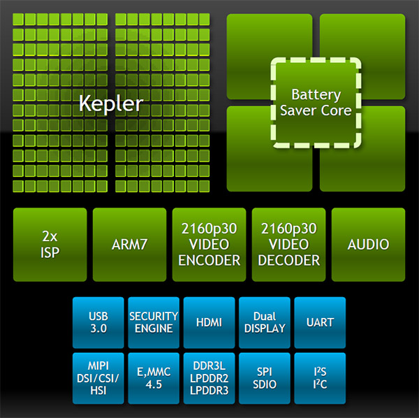
Before we dive deeper into the Tegra K1 SoC’s subsystems, here’s an overview that looks a lot like what Nvidia presented when it launched Tegra 4.
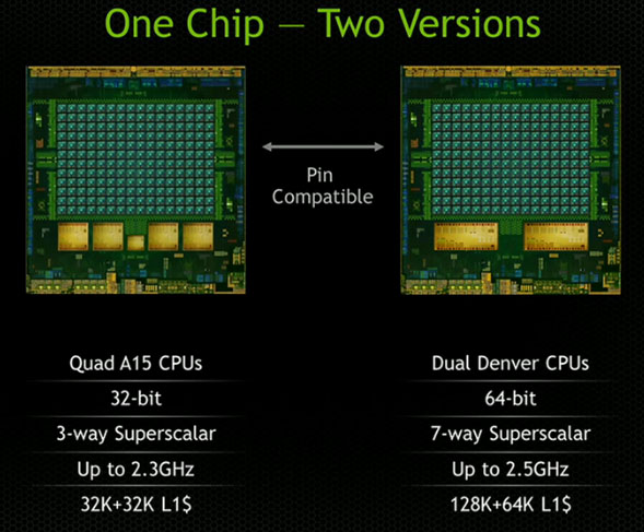
Last night, Nvidia announced two versions of Tegra K1. The first version we knew was coming. That's what you see above. It's a 4+1 architecture consisting of four “big” Cortex-A15 cores and one Cortex-A15 “battery saver” core with 2 MB of L2 cache. The second version was a surprise. It's pin-compatible, but instead sports two 64-bit cores based on the company's Project Denver, first discussed back in 2011.
Get Tom's Hardware's best news and in-depth reviews, straight to your inbox.
Nvidia wouldn't answer any of our questions about the Denver-based model, except to say that it introduces 64-bit support, is a much wider seven-way superscalar design (versus Cortex-A15's three-way), runs at up to 2.5 GHz, features 128 KB of L1 instruction and 64 KB of L1 data cache, and of course is a custom design based on the ARMv8 architecture.
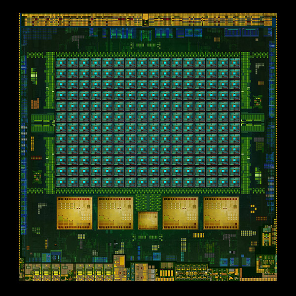
The GPU is significantly overhauled, no longer composed of separate programmable vertex and pixel shaders, but rather built using the same Kepler architecture prevalent across Nvidia’s GeForce family. Tegra K1 sports 192 CUDA cores, and of course, because they’re so fundamentally different, you can’t compare them to Tegra 4’s 24 vertex and 48 pixel shaders. Implementing Kepler in the Tegra K1 does enable OpenGL ES 3.0 support though, which Tegra 4 was notably missing. DirectX 11-, OpenGL 4.4-, OpenCL 1.1-, and CUDA-based apps will also run on Tegra K1.
Imaging was clearly a focus of the Tegra 4 launch, although I’d argue that we still haven’t seen the real potential of Nvidia’s ISP. Nevertheless, the company makes significant improvements to this subsystem for Tegra K1, boosting peak throughput to 1.2 gigapixels/s (up from a claimed 350 megapixels/s) and supporting sensors as large as 100 megapixels.
Tegra 4’s fixed-function video encode and decode pipelines were limited to 2160p at 24 FPS; Tegra K1 pushes that to 2160p support at 30. Whereas Qualcomm’s Snapdragon 805 is expected to support HEVC decoding in hardware, Nvidia makes no mention of acceleration in Tegra K1, unfortunately.
The SoC’s display controller is improved. Nvidia says Tegra K1 supports the same 4x2 DSI, but also includes eDP, LVDS, and HDMI 1.4b support to drive up to 4K panels and 4K external devices. Tegra 4 required an external DSI-to-eDP bridge chip for DisplayPort connectivity.
Tegra K1 is manufactured using TSMC’s 28 nm HPM process, similar to Qualcomm’s Snapdragon 800, which already powers a number of shipping devices. In comparison, Tegra 4 utilized 28 nm HPL, a high-performance, low-leakage technology not as ideal for mobile SoCs.
Current page: A Little Bit Of The PC In Your Next Tablet?
Next Page Tegra K1’s CPU: An Updated 4+1 Cortex-A15 Design-
RupertJr "Approx. Comparison To Both Last-Gen Consoles"Reply
Why don't you update the graph title to "Prev Gen Consoles" since last gen consoles has 1.23 TFLOPS (XBOX One) and 1.84 TFLOPS (PS4) performance difference to this K1 chip is huge. It looks like NVidia will loose another battle... -
renz496 Reply12372657 said:Where is the maxwell stuff did they not even address it yesterday? WTF
most likely they will talk about it when the actual gpu is close to release. -
Wisecracker ReplyAt least in theory, Tegra K1 could be on par with those previous-generation systems ...
AMD does it. Intel, too. But ...
When it comes to over-the-top hype, embellishment and hyperbole, nVidia is the king.
-
ZolaIII @ Rupert JrReply
Well multiplied 3x & with higher memory bandwidth you are there.
1.5x Maxwell & 2x cores (28nm to 16-14nm).
Hyper memory cube.
All this in 2015. -
RupertJr @ZolaIIIReply
but what you are assuming does not exists nowadays and maybe until years...
where will be other chips at that time? -
dragonsqrrl "in fact, the first Maxwell-powered discrete GPUs are expected in the next few weeks"Reply
Excellent. -
InvalidError Reply
Well, they are right on at least one thing: 2014's SoCs are now about on par with high-end components from ~7 years ago or mid-range gaming PCs from ~5 years ago and are managing to do so on a 2-3W power budget, which is rightfully impressive IMO.12373063 said:It looks like NVidia will loose another battle...
If SoCs continue improving at this pace while PCs remain mostly stagnant, the performance gap between SoCs and mainstream PCs will be mostly gone by the time 2015 is over. -
Shankovich I'm assuming this SoC will run at around 15 watts. With 192 CUDA cores and DDR3 LP, your max output will probably be somewhere around 180 GFLOPS. Yes yes it CAN do the same effects as consoles and PC, so what? If the Game Cube had DX 11.2 api running on it, it could as well, but obviouslt it coiuldn't put too much on the screen. This will be the same deal with the K1.Reply
It's cool, I like it, don't get me wrong, but the stuff they're saying, though technically correct, is so misleading to about 90% of the market. People are going to think they have PS4's in their hand when in reality they have half a xbox 360 with up to date API's running on it.


