Evidence mounts that TSMC won't adopt next-gen EUV chipmaking tools until 1nm debuts in the 2030 timeframe
2030 and onwards?

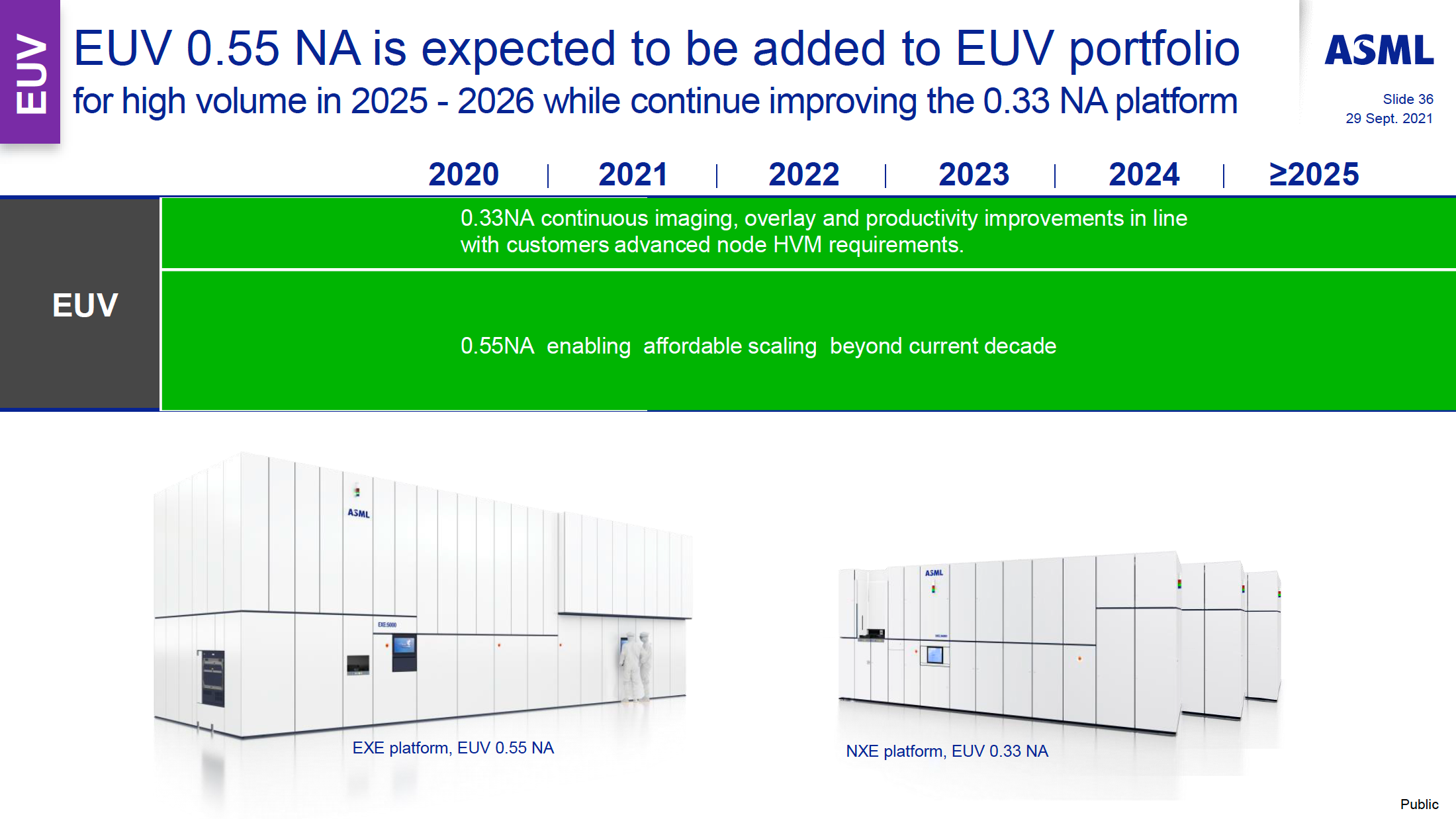
Unlike Intel, TSMC hasn't announced when it plans to start using ASML's next-gen High-NA extreme ultraviolet (EUV) chipmaking tools, which has naturally led to plenty of speculation about its intentions. A month ago, an analyst wrote in a note to clients that TSMC would wait to use High-NA tools until it begins producing its 1nm process technology. This week, DigiTimes added its voice to that story with its own sources at fab toolmakers confirming that TMCS would wait until 1nm to use the next-gen tool, though we do have to caution that TSMC hasn't officially announced the news.
TSMC's delay could boil down to cost concerns. Analysts from SemiAnalysis believe that TSMC will only begin to use High-NA EUV systems with its 1nm-class process technology (known as A10), which, assuming TSMC retains its current cadence of introducing new nodes, would happen sometime in 2029 – 2030 (production start – availability).
Intel is set to use High-NA EUV tools for its post-18A process technology, which probably means it will begin using them in the 2026 – 2027 range (though Intel has not formally confirmed the timeframe). Meanwhile, all of the leading makers of logic and memory have purchased High-NA EUV tools for their research and development (R&D) efforts but have not set any deployment schedules publicly.
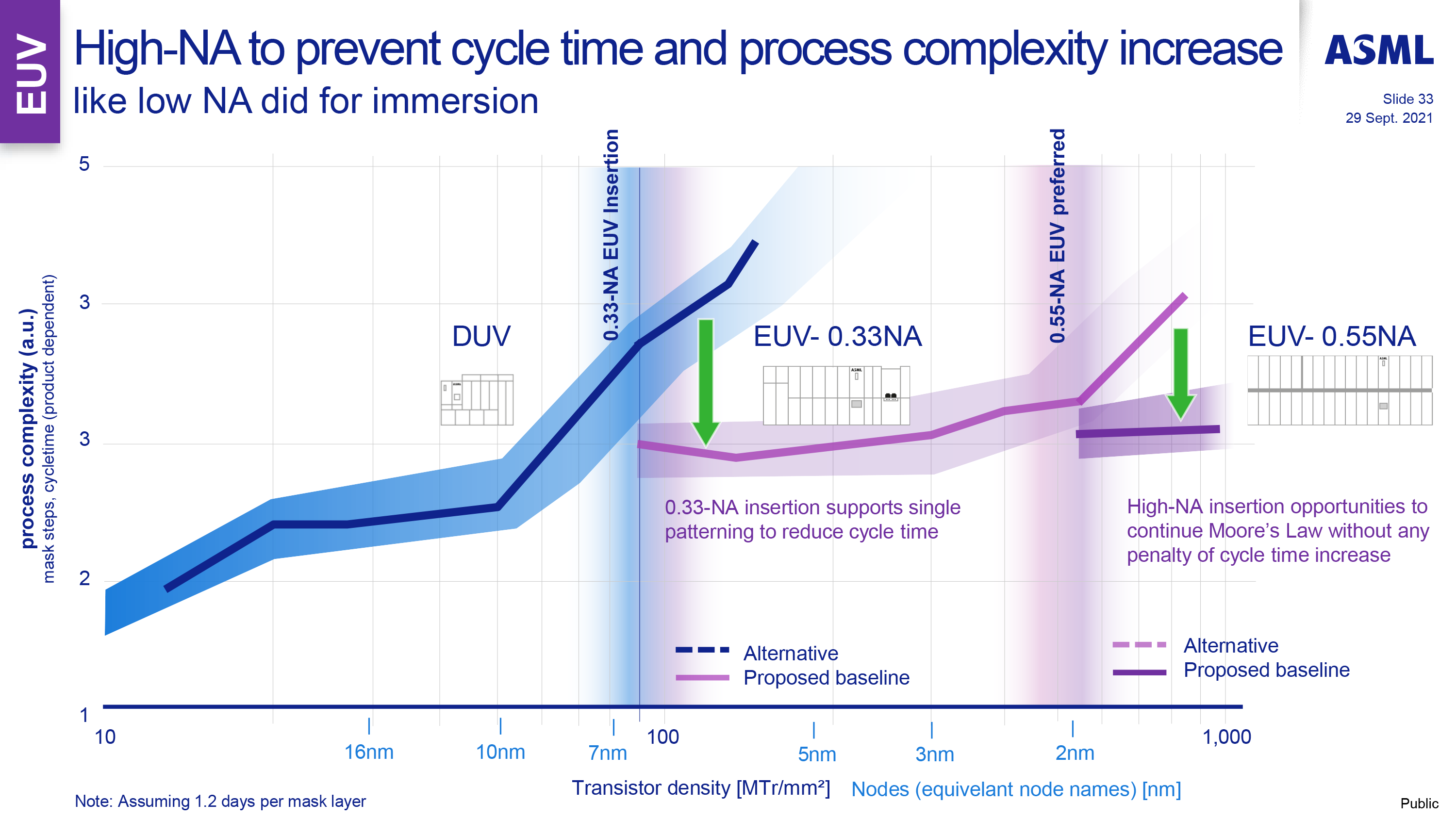
High-NA EUV lithography tools allow the achievement of 8nm dimensions with a single exposure, significantly improving over the 13nm featured by existing Low-NA EUV tools. However, not all chipmakers are in a rush to deploy these chipmaking tools commercially because existing EUV systems can achieve an 8nm resolution with double patterning, ostensibly for lower overall cost. High-NA EUV tools are also exceedingly expensive and require substantial changes to existing fabrication facilities to accommodate their immense size.
One thing to keep in mind is that plans tend to change based on the performance of existing technologies as well as other market factors. That said, while it might not look like TSMC is set to insert High-NA EUV tools any time soon, the plans aren't official, and if they were, the company's plans are always subject to change.
Get Tom's Hardware's best news and in-depth reviews, straight to your inbox.

Anton Shilov is a contributing writer at Tom’s Hardware. Over the past couple of decades, he has covered everything from CPUs and GPUs to supercomputers and from modern process technologies and latest fab tools to high-tech industry trends.
-
The Historical Fidelity It just seems that a 5nm decrease in feature size capability is not worth the cost increase of the NA tool investment until it’s absolutely necessary. Which btw, NA EUV is kind of in the same ballpark as immersion lithography for DUV in that dry DUV has a single pattern feature size limit of 65nm and immersion DUV of 45nm which is a similar reduction scale as EUV 13nm to NA 8nm.Reply -
jkflipflop98 Depends on how many wafers you're making. The reduction in process steps is well worth it. Higher overall throughput and less impact to yields make this a no-brainer.Reply -
The Historical Fidelity Reply
It’s TSMC so a lot of wafers and they know better than anyone whether it makes sense to double pattern vs invest in $500,000,000 tools. They chose double pattern for a reason.jkflipflop98 said:Depends on how many wafers you're making. The reduction in process steps is well worth it. Higher overall throughput and less impact to yields make this a no-brainer. -
kjfatl This so reminds me of what Intel did about 10 years ago when they decided to due multiple patterning instead of investing in EUV. It took them from the undisputed #1 player in the market to #3. The expected path for TSMC would be to set up at least one fab with high NA EUV equipment so they can continue to develop their processes and go into high volume production on a few bleeding edge products. It looks like they have decided to hand the torch back to Intel.Reply -
zodiacfml wow. If TSMC does not buy more NA EUV than Intel then all these years of Intel decline was intentional! Intel is taking the cutting edge semicon back. I could smell this from years ago! It is not like Intel could get behind TSMC as there were no signs of Intel mistakes or miss steps. the truth is, process node superiority is just buying the latest ASML equipment and hope you have volumes to pay for it.Reply -
The Historical Fidelity Reply
More like Intel knows that their processes are not on par with TSMC efficiency wise so they must utilize every advantage they can to control transistor leakage.zodiacfml said:wow. If TSMC does not buy more NA EUV than Intel then all these years of Intel decline was intentional! Intel is taking the cutting edge semicon back. I could smell this from years ago! It is not like Intel could get behind TSMC as there were no signs of Intel mistakes or miss steps. the truth is, process node superiority is just buying the latest ASML equipment and hope you have volumes to pay for it. -
The Historical Fidelity Reply
It’s apples to oranges, going from minimum feature sizes of 45nm with single pattern immersion DUV to 13nm single pattern EUV is much greater than from EUV 13nm to 8nm single pattern High NA EUV. IE Intel chose not to upgrade resolution by 3.5x vs TSMC choosing to not upgrade resolution by 0.6x. It won’t be anything that greatly affects TSMC’s leadership.kjfatl said:This so reminds me of what Intel did about 10 years ago when they decided to due multiple patterning instead of investing in EUV. It took them from the undisputed #1 player in the market to #3. The expected path for TSMC would be to set up at least one fab with high NA EUV equipment so they can continue to develop their processes and go into high volume production on a few bleeding edge products. It looks like they have decided to hand the torch back to Intel. -
phead128 Reply
They all have access to the same ASML EUV equipment, just TSMC is superior at systems integration and efficiency, so they can secure the volume orders from Apple. Intel is inferior in efficiency and yield, even with the same EUV tools, they can't get good cost-per-unit yields to compete with TSMC. They hope to compensate their weakness with more accurate overlays to improve performance, doesn't mean their cost efficiency will be the same.zodiacfml said:wow. If TSMC does not buy more NA EUV than Intel then all these years of Intel decline was intentional! Intel is taking the cutting edge semicon back. I could smell this from years ago! It is not like Intel could get behind TSMC as there were no signs of Intel mistakes or miss steps. the truth is, process node superiority is just buying the latest ASML equipment and hope you have volumes to pay for it.
