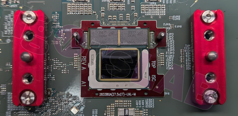
Intel's Lunar Lake MX mobile processor pictured, with LPDDR5X memory on board
Intel reportedly worked very closely with Microsoft to optimize Windows for Lunar Lake.

Igor's Lab this week published an image of Intel's Lunar Lake MX processor, which proves that PC makers are hard at work developing notebooks with LNL CPUs inside. The picture also confirms that Lunar Lake uses a multi-chiplet design and comes with on-package LPDDR5X memory to maximize its performance.
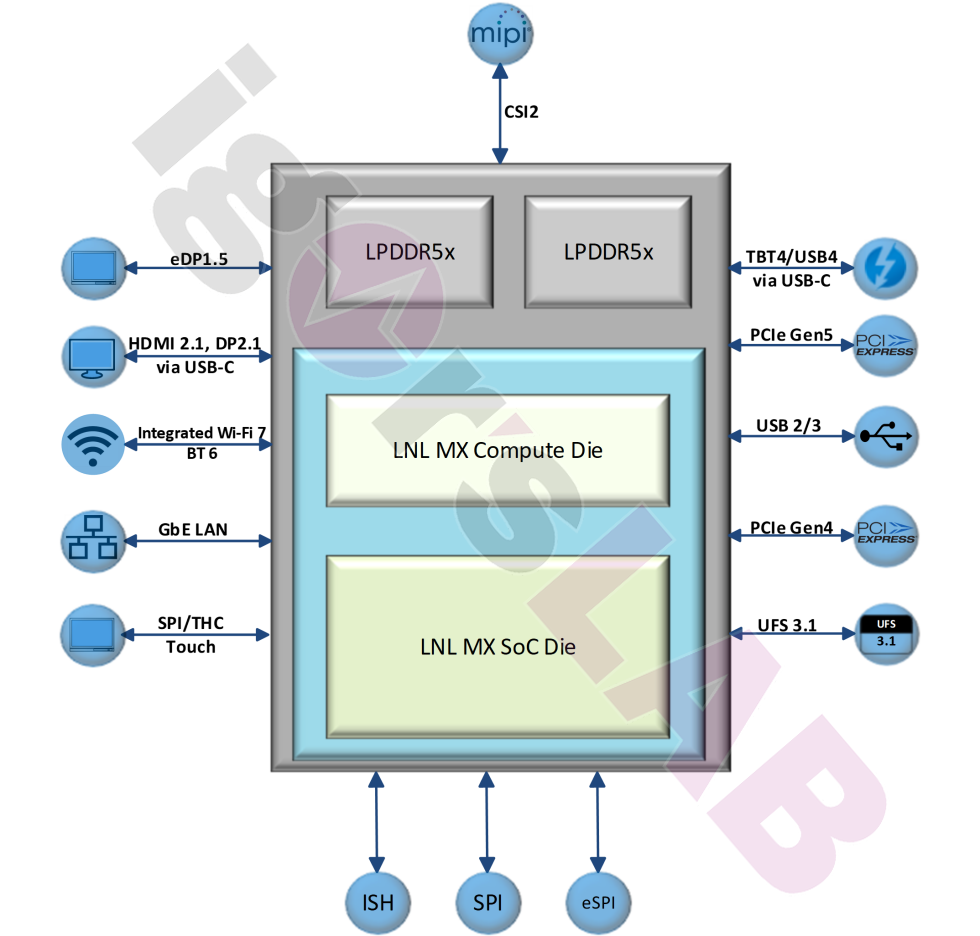
Intel expects its Lunar Lake processors to offer significant improvements in the performance efficiency of its platforms due to microarchitectural innovations. The Lunar Lake MX's compute tile reportedly packs eight general-purpose cores — four high-performance Lion Cove cores and four energy-efficient Skymont cores — to offer the right balance between performance and power consumption. The compute tile also reportedly packs an integrated GPU featuring 64 Xe2 Execution Units (EUs) based on the Battlemage architecture. The system-on-chip also has a six-tile NPU 4.0 AI accelerator and a system-on-chip tile that connects to the main tile using Intel's Foveros technology and packs various I/O features.
A notable shift in Intel's approach, in the case of Lunar Lake MX, is the use of TSMC's N3B manufacturing technology for the compute tile. This move marks a significant change from Intel's traditional reliance on in-house manufacturing for its high-end chips. It is noteworthy that Intel originally planned to use its 18A (1.8nm-class) fabrication process for Lunar Lake-series CPUs, but 18A will not be ready for production until late 2024, whereas TSMC's N3B is used for mass production today.
Interestingly, Igor's Lab further claims that Intel's Lunar Lake MX processors have been co-developed in close collaboration with Microsoft, focusing on enhancing the interaction between software and hardware. This collab indicates that users could expect a better use of CPU capabilities, particularly in systems running the latest and upcoming versions of Microsoft's operating systems.
Intel's Lunar Lake MX is targeted mainly at thin-and-light laptops and is expected to feature 16GB or 32GB of LPDDR5X-8533 memory directly integrated into the package. This design choice aims to minimize the platform's size and enhance performance. According to Intel's projections from slides that were leaked several months ago, the Lunar Lake MX configuration is estimated to save between 100 to 250 square millimeters of space compared to conventional designs where the memory is separate from the CPU package.
Depending on the power target, the Lunar Lake platform will support 8W fanless and 17W – 30W actively cooled designs.
Get Tom's Hardware's best news and in-depth reviews, straight to your inbox.

Anton Shilov is a contributing writer at Tom’s Hardware. Over the past couple of decades, he has covered everything from CPUs and GPUs to supercomputers and from modern process technologies and latest fab tools to high-tech industry trends.
-
Notton I am guessing it uses 2x 64Gb (8GB) or 128Gb (16GB) LPDDR5x densities?Reply
I wonder why they don't have an in-between size.
The 96Gb (12GB) density exists on catalogue for both Samsung and Micron, last I checked. -
thestryker Reply
That's what every leak has indicated so far.Notton said:I am guessing it uses 2x 64Gb (8GB) or 128Gb (16GB) LPDDR5x densities?
Nobody has been using them which really confuses me. I believe they've been listed as mass production for a while so the availability should be there. I'd primarily been watching the handheld space, because 24GB total capacity is perfect and shouldn't cost significantly more than a 16GB implementation.Notton said:I wonder why they don't have an in-between size.
The 96Gb (12GB) density exists on catalogue for both Samsung and Micron, last I checked. -
cyrusfox Reply
Why should they do that? HBM is 2-3x more expensive, will the greater bandwidth provided be utilized to offset the added cost?newtechldtech said:This approach should use HBM technology and not DDR technology
As on package DDR is already much faster than off chip DDR, there is less of a performance advantage for HBM.
Apple which has been doing on package memory since the M1 continues to utilize DDR standard (they started with LPDDR4X and quickly moved to LPDDR5 which they are still using on the M3). The bandwidth/latency advantage is tunable with on package DDR (High speed and large bit bus width). Commodity parts sure makes more sense to me here. HBM only is worth the cost if the application/use warrants it (H100, A100, B100/B200,etc...). -
Amdlova If they don't put 8 gb on the chip.and says that is enough like apple does it's good for me. Hbm it's just a dream... ddr5 just side by side with the cpu it's too good for u Poor consumersReply -
newtechldtech Reply
it is worth it to use HBM in laptops for onboard GPU ... the ARC GPU will run faster.cyrusfox said:Why should they do that? HBM is 2-3x more expensive, will the greater bandwidth provided be utilized to offset the added cost?
As on package DDR is already much faster than off chip DDR, there is less of a performance advantage for HBM.
Apple which has been doing on package memory since the M1 continues to utilize DDR standard (they started with LPDDR4X and quickly moved to LPDDR5 which they are still using on the M3). The bandwidth/latency advantage is tunable with on package DDR (High speed and large bit bus width). Commodity parts sure makes more sense to me here. HBM only is worth the cost if the application/use warrants it (H100, A100, B100/B200,etc...). -
JayNor "It is noteworthy that Intel originally planned to use its 18A (1.8nm-class) fabrication process for Lunar Lake-series CPUs..."Reply
Whatever process it is using, the decision was likely made years ago according to the most recent earnings call comments by PG.

