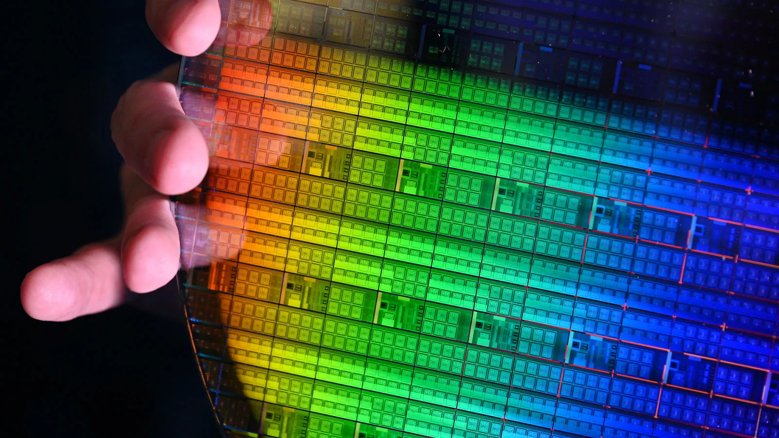
Given how SRAM-intensive modern designs are, SRAM cell size and density are major characteristics of new fabrication technologies. Apparently, the SRAM density of Intel's 18A manufacturing process (1.8nm-class) is considerably lower than that of TSMC's N2 (2nm-class), and is closer to TSMC's N3, according to the ISSCC 2025 Advance Program. Still, Intel's 18A could have other major advantages over N2.
Intel's 18A fabrication process features a high-density SRAM bit cell size of 0.021 µm^2 (therefore achieving an SRAM density of approximately 31.8 Mb/mm^2), which is a major improvement compared to a high-density SRAM bit cell size of 0.024 µm^2 in Intel 4, but aligns with what TSMC's N3E and N5 offer. By contrast, TSMC's N2 manufacturing technology shrinks HD SRAM bit cell size to around 0.0175 µm^2, enabling SRAM density of 38 Mb/mm^2.
| Row 0 - Cell 0 | Intel 4 | Intel 18A | N3 | N3E | N2 |
| SRAM Density | 27.825 Mb/mm^2 | 31.8 Mb/mm^2 | 33.55 Mb/mm^2 | 31.8 Mb/mm^2 | 38 Mb/mm^2 |
| SRAM Cell Size | 0.0240 µm^2 | 0.0210 µm^2 | 0.0199 µm^2 | 0.021 µm^2 | 0.0175 µm^2 |
| HVM | Row 3 - Cell 1 | Row 3 - Cell 2 | Q4 2022 | Q4 2023 | H2 2025 |
Speaking of Intel's 18A, this node has two major advantages over its predecessors: GAA transistors and a backside power delivery network (BSPDN). BSPDN not only promises to improve power delivery to transistors, thereby improving performance efficiency for some designs but also enables designers to make them smaller, thus increasing logic density.
Although modern chip designs use plenty of SRAM, and its density is crucial for node-to-node scaling, logic density is more important than HDC SRAM density. For now, we cannot compare this metric for Intel's 18A and TSMC's N2. Furthermore, logic density is hard to estimate, as each process technology has high-density, high-performance, and low-power libraries that are usually mixed and matched within a single design. As for logic density for an abstract processor, Intel and TSMC have yet to disclose it.
One of the hardest things to scale with modern process technologies is SRAM density due to the intricacies of its design, operational requirements for stability and reliability, and increased variability at smaller nodes. That said, it is not surprising that some modern technologies may feature larger SRAM cell sizes compared to other production nodes.
