IBM, Samsung Develop VTFET Semiconductor Design for the Future
Vertical-Transport Nanosheet Field Effect Transistors could change the industry for years to come.

IBM and Samsung have announced a new semiconductor manufacturing design architecture they're calling Vertical-Transport Nanosheet Field Effect Transistors (VTFET for short). The new manufacturing design principle promises to allow for further transistor density increases, as well as doubled performance at the same power consumption, or 85% higher energy efficiency for the same overall performance compared to a similarly-scaled finFET alternative.


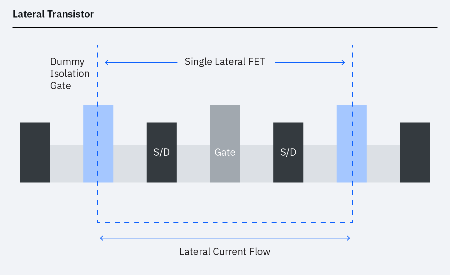
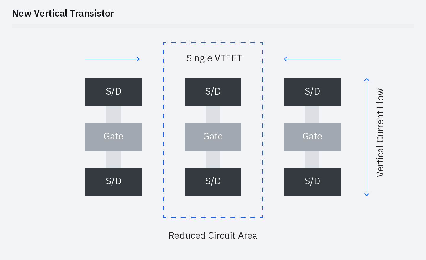
One reason improving transistor density is an increasingly difficult task is that typically, transistors are arranged and laid out in a wafer in a horizontal fashion. The problem here is that transistor components take up much more surface area on the chip than they would if they were vertically-arranged. In existing processes, transistor density increases have been focused on reducing the size of these components, such as spacer, gate and wire pitches. However, these fundamental units (which also include insulating elements between transistors) all still have to fit within the Contacted Gate Pitch (CGP) - the minimum area required for a functioning transistor to be laid out. But what if transistors were actually designed vertically, instead of horizontally?

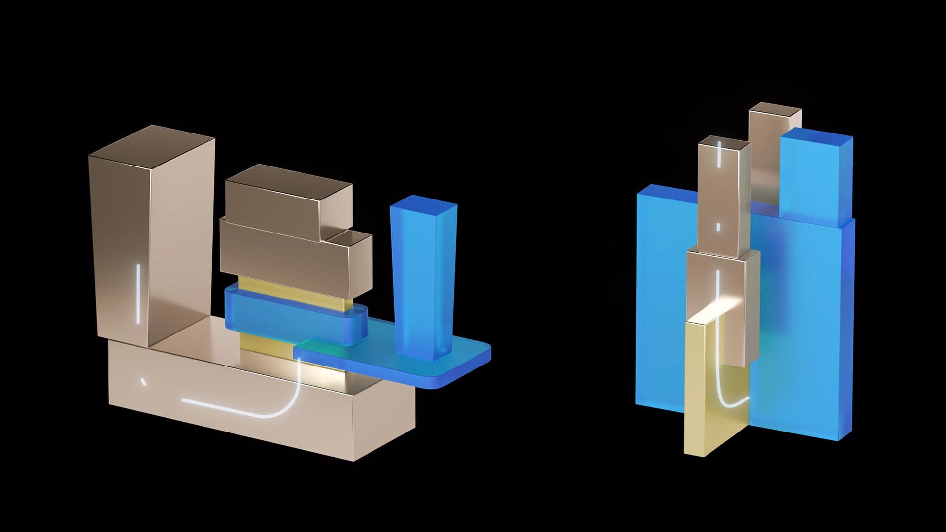
VTFET does exactly that; it's a new way to design transistors that actually places them perpendicularly to the wafer, allowing them to scale on the Z axis instead of taking up valuable wafer floor space. This allows manufacturers to reduce the number of components required for a functional transistor (they can now lose the inter-transistor insulators), which in turn allows for them to be placed closer together. Current naturally flows vertically in this arrangement, instead of the common horizontal current flow that's currently employed. Freed from the constraints of horizontal scaling, researchers can now independently optimize transistor components - spacer, contact and gate sizes, for instance - for power and performance characteristics of the chip. The decades-old tradeoff process between balancing all those components in the relatively constrained quarters of horizontal layouts now gets a much-needed breather.
Article continues belowThese additional engineering options are a big element of the doubled performance or 85% higher efficiency of VTFET transistors. TSMC, for example, achieved much smaller benefits from its transitioning between 7 nm and 5 nm technologies - TSMC quoted a 20% performance improvement at the same power or a 40% maximum energy efficiency improvement. "Simply" rearranging transistor layouts vertically can thus be more impactful than even node changes - and VTFET transistors can of course also be further miniaturized with advancements in manufacturing.
It remains to be seen on which technologies the industry will settle along the way to sub-nanometer transistor size and densities. Whether via VTFETs or CASFETs (which have brought about quantum computing design principles to transistor design) or another technological solution, one thing is certain: not even physics can stand in the way of our technological progress.
Manufacturers have been struggling to keep Moore's Law alive for years now, with multiple solutions to the ever more difficult transistor miniaturization problem. Intel's continuous delays of its 10 nm node before finally managing to bring its SuperFin design to bear come to mind as one such example. The fact that even Intel, the largest semiconductor manufacturer - and with as deep investment pockets as it has - stumbled on this road to such a market upheaval is enough to showcase just exactly how critical these manufacturing improvements are for success.
Get Tom's Hardware's best news and in-depth reviews, straight to your inbox.

Francisco Pires is a freelance news writer for Tom's Hardware with a soft side for quantum computing.
-
BillyBuerger Reply...not even physics can stand in the way of our technological progress.
Oh, so they're using magic now to create transistors instead of science. Interesting... -
Endymio " "Simply" rearranging transistor layouts vertically can thus be more impactful than even node changes..."Reply
Vertical manufacturing at this scale is not a "simple" rearrangement, and given the new transistor architecture. this change is considerably more involved than a mere node shrink. -
InvalidError This is basically an evolution of VFET.Reply
I'd imagine gate-all-around is much easier to achieve with simple concentric vertical gates and P/N channels than building fins or stacks across several layers. -
Endymio Reply
On the contrary, the article states this architecture is "free from the constraints" of the traditional difficulties of increasing transistor densities, then moves immediately on to discuss its benefits. Nowhere are the complexities of a new transistor design even touched upon, and in fact are summarized merely as no more than a "design principle", rather than an entirely new architecture.Francisco Alexandre Pires said:The entire article is all about how it isn't "simple"; the "simply" is even within quotation marks, implying that it itself is an oversimplification of what had been previously described. -
InvalidError Reply
Well, if you use Gate-All-Around as a starting point, all of the extra complexities from needing to dope semiconductor layers other than the silicon substrate are already there. Vertical channel transistors are quite possibly easier to make using fewer total fab steps than multi-channel stacked GAA FETs.Endymio said:Nowhere are the complexities of a new transistor design even touched upon, and in fact are summarized merely as no more than a "design principle", rather than an entirely new architecture.